DF2328BVF25V Renesas Electronics America, DF2328BVF25V Datasheet - Page 402
DF2328BVF25V
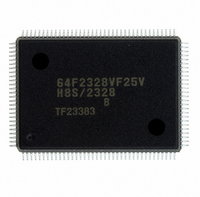
Manufacturer Part Number
DF2328BVF25V
Description
IC H8S MCU FLASH 256K 128QFP
Manufacturer
Renesas Electronics America
Series
H8® H8S/2300r
Datasheets
1.HEWH8E10A.pdf
(19 pages)
2.D12312SVTE25V.pdf
(341 pages)
3.D12322RVF25V.pdf
(1304 pages)
Specifications of DF2328BVF25V
Core Processor
H8S/2000
Core Size
16-Bit
Speed
25MHz
Connectivity
SCI, SmartCard
Peripherals
DMA, POR, PWM, WDT
Number Of I /o
87
Program Memory Size
256KB (256K x 8)
Program Memory Type
FLASH
Ram Size
8K x 8
Voltage - Supply (vcc/vdd)
2.7 V ~ 3.6 V
Data Converters
A/D 8x10b; D/A 2x8b
Oscillator Type
Internal
Operating Temperature
-20°C ~ 75°C
Package / Case
128-QFP
For Use With
EDK2329 - DEV EVALUATION KIT H8S/2329
Lead Free Status / RoHS Status
Lead free / RoHS Compliant
Eeprom Size
-
Other names
HD64F2328BVF25V
Available stocks
Company
Part Number
Manufacturer
Quantity
Price
Company:

Part Number:
DF2328BVF25V
Manufacturer:
Renesas Electronics America
Quantity:
10 000


Section 9 I/O Ports
Pin
P2
TMCI
Rev.6.00 Sep. 27, 2007 Page 370 of 1268
REJ09B0220-0600
3
/PO
0
3
/TIOCD
3
/
Selection Method and Pin Functions
This pin is used as the 8-bit timer external clock input pin when an external
clock is selected with bits CKS2 to CKS0 in TCR0.
The pin function is switched as shown below according to the combination of
the TPU channel 3 setting (by bits MD3 to MD0 in TMDR3, bits IOD3 to IOD0
in TIOR3L, and bits CCLR2 to CCLR0 in TCR3), bit NDER3 in NDERL, and bit
P23DDR.
Note: * TIOCD
TPU Channel
3 Setting
P23DDR
NDER3
Pin function
TPU Channel
3 Setting
MD3 to MD0
IOD3 to IOD0
CCLR2 to
CCLR0
Output
function
3
input when MD3 to MD0 = B'0000, and IOD3 to IOD0 = B'10xx.
B'0000
B'0100
B'1xxx
(2)
—
—
B'0000
Table Below (1)
TIOCD
B'0001 to
B'0011
B'0101 to
B'0111
compare
Output
output
(1)
—
—
—
3
output
B'0010
(2)
—
—
—
TMCI
0
input
B'xx00
input
P2
(2)
—
—
—
0
3
Table Below (2)
TIOCD
Other than B'xx00
mode 2
B'0011
output
output
Other
B'110
PWM
than
P2
(1)
1
0
3
3
input *
x: Don’t care
output
B'110
PO
(2)
—
1
1
3
Related parts for DF2328BVF25V
Image
Part Number
Description
Manufacturer
Datasheet
Request
R

Part Number:
Description:
KIT STARTER FOR M16C/29
Manufacturer:
Renesas Electronics America
Datasheet:

Part Number:
Description:
KIT STARTER FOR R8C/2D
Manufacturer:
Renesas Electronics America
Datasheet:

Part Number:
Description:
R0K33062P STARTER KIT
Manufacturer:
Renesas Electronics America
Datasheet:

Part Number:
Description:
KIT STARTER FOR R8C/23 E8A
Manufacturer:
Renesas Electronics America
Datasheet:

Part Number:
Description:
KIT STARTER FOR R8C/25
Manufacturer:
Renesas Electronics America
Datasheet:

Part Number:
Description:
KIT STARTER H8S2456 SHARPE DSPLY
Manufacturer:
Renesas Electronics America
Datasheet:

Part Number:
Description:
KIT STARTER FOR R8C38C
Manufacturer:
Renesas Electronics America
Datasheet:

Part Number:
Description:
KIT STARTER FOR R8C35C
Manufacturer:
Renesas Electronics America
Datasheet:

Part Number:
Description:
KIT STARTER FOR R8CL3AC+LCD APPS
Manufacturer:
Renesas Electronics America
Datasheet:
Part Number:
Description:
KIT STARTER FOR RX610
Manufacturer:
Renesas Electronics America
Datasheet:

Part Number:
Description:
KIT STARTER FOR R32C/118
Manufacturer:
Renesas Electronics America
Datasheet:

Part Number:
Description:
KIT DEV RSK-R8C/26-29
Manufacturer:
Renesas Electronics America
Datasheet:

Part Number:
Description:
KIT STARTER FOR SH7124
Manufacturer:
Renesas Electronics America
Datasheet:

Part Number:
Description:
KIT STARTER FOR H8SX/1622
Manufacturer:
Renesas Electronics America
Datasheet:

Part Number:
Description:
KIT DEV FOR SH7203
Manufacturer:
Renesas Electronics America
Datasheet: