DF2328BVF25V Renesas Electronics America, DF2328BVF25V Datasheet - Page 418
DF2328BVF25V
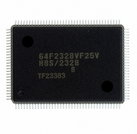
Manufacturer Part Number
DF2328BVF25V
Description
IC H8S MCU FLASH 256K 128QFP
Manufacturer
Renesas Electronics America
Series
H8® H8S/2300r
Datasheets
1.HEWH8E10A.pdf
(19 pages)
2.D12312SVTE25V.pdf
(341 pages)
3.D12322RVF25V.pdf
(1304 pages)
Specifications of DF2328BVF25V
Core Processor
H8S/2000
Core Size
16-Bit
Speed
25MHz
Connectivity
SCI, SmartCard
Peripherals
DMA, POR, PWM, WDT
Number Of I /o
87
Program Memory Size
256KB (256K x 8)
Program Memory Type
FLASH
Ram Size
8K x 8
Voltage - Supply (vcc/vdd)
2.7 V ~ 3.6 V
Data Converters
A/D 8x10b; D/A 2x8b
Oscillator Type
Internal
Operating Temperature
-20°C ~ 75°C
Package / Case
128-QFP
For Use With
EDK2329 - DEV EVALUATION KIT H8S/2329
Lead Free Status / RoHS Status
Lead free / RoHS Compliant
Eeprom Size
-
Other names
HD64F2328BVF25V
Available stocks
Company
Part Number
Manufacturer
Quantity
Price
Company:

Part Number:
DF2328BVF25V
Manufacturer:
Renesas Electronics America
Quantity:
10 000


Section 9 I/O Ports
9.6.3
Port 5 pins also function as SCI I/O pins (TxD
(ADTRG), interrupt input pins (IRQ
BREQO). Port 5 pin functions are shown in table 9.10.
Table 9.10 Port 5 Pin Functions
Pin
P5
IRQ7/WAIT/
BREQO
P5
Rev.6.00 Sep. 27, 2007 Page 386 of 1268
REJ09B0220-0600
3
2
/ADTRG/
/SCK
2
/IRQ
Pin Functions
6
Selection Method and Pin Functions
The pin function is switched as shown below according to the combination of
the operating mode, bits TRGS1 and TRGS0 in the A/D control register
(ADCR), and bits IRQPAS, WAITE, WAITPS, BREQOE, BREQOPS, and
P53DDR.
Notes: 1. ADTRG input when TRGS0 = TRGS1 = 1.
The pin function is switched as shown below according to the combination of
bit C/A in the SCI2 SMR, bits CKE0 and CKE1 in SCR, and bits IRQPAS and
P52DDR.
Note: * IRQ
Operating mode
[BREQOE ·
BREQOPS]
[WAITE ·
WAITPS]
P53DDR
Pin function
CKE1
C/A
CKE0
P52DDR
Pin function
2. IRQ
6
input when IRQPAS = 1.
7
4
input when IRQPAS = 1.
to IRQ
input
input pin
P5
pin
0
P5
3
0
0
2
7
output
), and bus control signal I/O pins (WAIT and
P5
2
pin
, RxD
1
0
3
output pin
0
P5
2
WAIT
input
Modes 4 to 6
, and SCK
0
1
pin
0
IRQ
2
IRQ
ADTRG input pin *
1
6
7
Setting
hibited
0
interrupt input pin *
interrupt input pin *
pro-
output pin
1
2
SCK
), the A/D converter input pin
—
1
BREQO
output
2
pin
—
0
1
output pin
1
Setting
hibited
SCK
pro-
2
—
1
—
—
1
2
input
P5
pin
0
Mode 7
3
input pin
SCK
—
—
—
—
—
1
output
P5
pin
1
2
3
Related parts for DF2328BVF25V
Image
Part Number
Description
Manufacturer
Datasheet
Request
R

Part Number:
Description:
KIT STARTER FOR M16C/29
Manufacturer:
Renesas Electronics America
Datasheet:

Part Number:
Description:
KIT STARTER FOR R8C/2D
Manufacturer:
Renesas Electronics America
Datasheet:

Part Number:
Description:
R0K33062P STARTER KIT
Manufacturer:
Renesas Electronics America
Datasheet:

Part Number:
Description:
KIT STARTER FOR R8C/23 E8A
Manufacturer:
Renesas Electronics America
Datasheet:

Part Number:
Description:
KIT STARTER FOR R8C/25
Manufacturer:
Renesas Electronics America
Datasheet:

Part Number:
Description:
KIT STARTER H8S2456 SHARPE DSPLY
Manufacturer:
Renesas Electronics America
Datasheet:

Part Number:
Description:
KIT STARTER FOR R8C38C
Manufacturer:
Renesas Electronics America
Datasheet:

Part Number:
Description:
KIT STARTER FOR R8C35C
Manufacturer:
Renesas Electronics America
Datasheet:

Part Number:
Description:
KIT STARTER FOR R8CL3AC+LCD APPS
Manufacturer:
Renesas Electronics America
Datasheet:
Part Number:
Description:
KIT STARTER FOR RX610
Manufacturer:
Renesas Electronics America
Datasheet:

Part Number:
Description:
KIT STARTER FOR R32C/118
Manufacturer:
Renesas Electronics America
Datasheet:

Part Number:
Description:
KIT DEV RSK-R8C/26-29
Manufacturer:
Renesas Electronics America
Datasheet:

Part Number:
Description:
KIT STARTER FOR SH7124
Manufacturer:
Renesas Electronics America
Datasheet:

Part Number:
Description:
KIT STARTER FOR H8SX/1622
Manufacturer:
Renesas Electronics America
Datasheet:

Part Number:
Description:
KIT DEV FOR SH7203
Manufacturer:
Renesas Electronics America
Datasheet: