DF2328BVF25V Renesas Electronics America, DF2328BVF25V Datasheet - Page 917
DF2328BVF25V
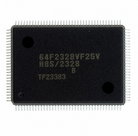
Manufacturer Part Number
DF2328BVF25V
Description
IC H8S MCU FLASH 256K 128QFP
Manufacturer
Renesas Electronics America
Series
H8® H8S/2300r
Datasheets
1.HEWH8E10A.pdf
(19 pages)
2.D12312SVTE25V.pdf
(341 pages)
3.D12322RVF25V.pdf
(1304 pages)
Specifications of DF2328BVF25V
Core Processor
H8S/2000
Core Size
16-Bit
Speed
25MHz
Connectivity
SCI, SmartCard
Peripherals
DMA, POR, PWM, WDT
Number Of I /o
87
Program Memory Size
256KB (256K x 8)
Program Memory Type
FLASH
Ram Size
8K x 8
Voltage - Supply (vcc/vdd)
2.7 V ~ 3.6 V
Data Converters
A/D 8x10b; D/A 2x8b
Oscillator Type
Internal
Operating Temperature
-20°C ~ 75°C
Package / Case
128-QFP
For Use With
EDK2329 - DEV EVALUATION KIT H8S/2329
Lead Free Status / RoHS Status
Lead free / RoHS Compliant
Eeprom Size
-
Other names
HD64F2328BVF25V
Available stocks
Company
Part Number
Manufacturer
Quantity
Price
Company:

Part Number:
DF2328BVF25V
Manufacturer:
Renesas Electronics America
Quantity:
10 000


Table 19.54 Software Protection
Item
SWE bit protection
Block specification
protection
Emulation protection •
19.26.3 Error Protection
In error protection, an error is detected when MCU runaway occurs during flash memory
programming/erasing, or operation is not performed in accordance with the program/erase
algorithm, and the program/erase operation is aborted. Aborting the program/erase operation
prevents damage to the flash memory due to overprogramming or overerasing.
If the MCU malfunctions during flash memory programming/erasing, the FLER bit is set to 1 in
FLMCR2 and the error protection state is entered. The FLMCR1, FLMCR2, EBR1, and EBR2
settings are retained, but program mode or erase mode is aborted at the point at which the error
occurred. Program mode or erase mode cannot be re-entered by re-setting the P1, P2, E1, or E2
bit. However, PV1, PV2, EV1, and EV2 bit setting is enabled, and a transition can be made to
verify mode.
Description
•
•
•
•
Clearing the SWE1 bit to 0 in FLMCR1 sets
the program/erase-protected state for area
H'000000 to H'03FFFF (Execute in on-chip
RAM, external memory, or addresses
H'040000 to H'07FFFF)
Clearing the SWE2 bit to 0 in FLMCR2 sets
the program/erase-protected state for area
H'040000 to H'07FFFF (Execute in on-chip
RAM, external memory, or addresses
H'000000 to H'03FFFF)
Erase protection can be set for individual
blocks by settings in erase block registers 1
and 2 (EBR1, EBR2).
Setting EBR1 and EBR2 to H'00 places all
blocks in the erase-protected state.
Setting the RAMS bit to 1 in the RAM
emulation register (RAMER) places all blocks
in the program/erase-protected state.
Rev.6.00 Sep. 27, 2007 Page 885 of 1268
Program
Yes
—
Yes
Functions
REJ09B0220-0600
Section 19 ROM
Erase
Yes
Yes
Yes
Related parts for DF2328BVF25V
Image
Part Number
Description
Manufacturer
Datasheet
Request
R

Part Number:
Description:
KIT STARTER FOR M16C/29
Manufacturer:
Renesas Electronics America
Datasheet:

Part Number:
Description:
KIT STARTER FOR R8C/2D
Manufacturer:
Renesas Electronics America
Datasheet:

Part Number:
Description:
R0K33062P STARTER KIT
Manufacturer:
Renesas Electronics America
Datasheet:

Part Number:
Description:
KIT STARTER FOR R8C/23 E8A
Manufacturer:
Renesas Electronics America
Datasheet:

Part Number:
Description:
KIT STARTER FOR R8C/25
Manufacturer:
Renesas Electronics America
Datasheet:

Part Number:
Description:
KIT STARTER H8S2456 SHARPE DSPLY
Manufacturer:
Renesas Electronics America
Datasheet:

Part Number:
Description:
KIT STARTER FOR R8C38C
Manufacturer:
Renesas Electronics America
Datasheet:

Part Number:
Description:
KIT STARTER FOR R8C35C
Manufacturer:
Renesas Electronics America
Datasheet:

Part Number:
Description:
KIT STARTER FOR R8CL3AC+LCD APPS
Manufacturer:
Renesas Electronics America
Datasheet:
Part Number:
Description:
KIT STARTER FOR RX610
Manufacturer:
Renesas Electronics America
Datasheet:

Part Number:
Description:
KIT STARTER FOR R32C/118
Manufacturer:
Renesas Electronics America
Datasheet:

Part Number:
Description:
KIT DEV RSK-R8C/26-29
Manufacturer:
Renesas Electronics America
Datasheet:

Part Number:
Description:
KIT STARTER FOR SH7124
Manufacturer:
Renesas Electronics America
Datasheet:

Part Number:
Description:
KIT STARTER FOR H8SX/1622
Manufacturer:
Renesas Electronics America
Datasheet:

Part Number:
Description:
KIT DEV FOR SH7203
Manufacturer:
Renesas Electronics America
Datasheet: