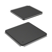
HD6417709SF133B Renesas Electronics America, HD6417709SF133B Datasheet - Page 129

HD6417709SF133B
Manufacturer Part Number
HD6417709SF133B
Description
IC SUPERH MPU ROMLESS 208LQFP
Manufacturer
Renesas Electronics America
Series
SuperH® SH7700r
Datasheet
1.D6417709SBP167BV.pdf
(809 pages)
Specifications of HD6417709SF133B
Core Processor
SH-3
Core Size
32-Bit
Speed
133MHz
Connectivity
EBI/EMI, FIFO, IrDA, SCI, SmartCard
Peripherals
DMA, POR, WDT
Number Of I /o
96
Program Memory Type
ROMless
Ram Size
16K x 8
Voltage - Supply (vcc/vdd)
1.65 V ~ 2.05 V
Data Converters
A/D 8x10b; D/A 2x8b
Oscillator Type
Internal
Operating Temperature
-20°C ~ 75°C
Package / Case
208-LQFP
Lead Free Status / RoHS Status
Contains lead / RoHS non-compliant
Eeprom Size
-
Program Memory Size
-
Available stocks
Company
Part Number
Manufacturer
Quantity
Price
Company:
Part Number:
HD6417709SF133B
Manufacturer:
RENESAS
Quantity:
79
Company:
Part Number:
HD6417709SF133B
Manufacturer:
Renesas Electronics America
Quantity:
10 000
Part Number:
HD6417709SF133B
Manufacturer:
RENESAS/瑞萨
Quantity:
20 000
Part Number:
HD6417709SF133B-V
Manufacturer:
RENESAS/瑞萨
Quantity:
20 000
Part Number:
HD6417709SF133BV
Manufacturer:
RENESAS/瑞萨
Quantity:
20 000
- Current page: 129 of 809
- Download datasheet (5Mb)
3.6.3
Invalidating Specific Entries: Specific TLB entries can be invalidated by writing 0 to the entry’s
V bit. When the A bit is 1, the VPN and ASID specified by the write data is compared to the VPN
and ASID within the TLB entry selected by the entry address and data is written to the matching
way. If no match is found, there is no operation. R0 specifies the write data and R1 specifies the
address.
Reading the Data of a Specific Entry: This example reads the data section of a specific TLB
entry. The bit order indicated in the data field in figure 3.14 (2) is read. R0 specifies the address
and the data section of a selected entry is read to R1.
3.7
The operations listed below must only be performed when the TLB is disabled or in the P1 or P2
area. Any subsequent operation that accesses the P0, P3, or U0 area must take place two or more
instructions after any of the below operations.
1. Change SR.MD or SR.BL
2. Execute the LDTLB instruction
3. Write to the memory-mapped TLB
4. Change MMUCR.
; R0=H'1547 381C
; MMUCR.IX=0
; VPN(31–17)=B'0001 0101 0100 011
; corresponding entry association is made from the entry selected by
; the VPN(16–12)=B'1 0011 index, the V bit of the hit way is cleared to
; 0,achieving invalidation.
MOV.L
; R1 H'F300 4300
MOV.L @R0,R1
Usage Examples
Usage Note
R0,@R1
R1=H'F201 3000
VPN(16-12)=B'00100
VPN(11–10)=B'10
Way 3
Rev. 5.00, 09/03, page 83 of 760
ASID=B'0001 1100
Related parts for HD6417709SF133B
Image
Part Number
Description
Manufacturer
Datasheet
Request
R

Part Number:
Description:
KIT STARTER FOR M16C/29
Manufacturer:
Renesas Electronics America
Datasheet:

Part Number:
Description:
KIT STARTER FOR R8C/2D
Manufacturer:
Renesas Electronics America
Datasheet:

Part Number:
Description:
R0K33062P STARTER KIT
Manufacturer:
Renesas Electronics America
Datasheet:

Part Number:
Description:
KIT STARTER FOR R8C/23 E8A
Manufacturer:
Renesas Electronics America
Datasheet:

Part Number:
Description:
KIT STARTER FOR R8C/25
Manufacturer:
Renesas Electronics America
Datasheet:

Part Number:
Description:
KIT STARTER H8S2456 SHARPE DSPLY
Manufacturer:
Renesas Electronics America
Datasheet:

Part Number:
Description:
KIT STARTER FOR R8C38C
Manufacturer:
Renesas Electronics America
Datasheet:

Part Number:
Description:
KIT STARTER FOR R8C35C
Manufacturer:
Renesas Electronics America
Datasheet:

Part Number:
Description:
KIT STARTER FOR R8CL3AC+LCD APPS
Manufacturer:
Renesas Electronics America
Datasheet:

Part Number:
Description:
KIT STARTER FOR RX610
Manufacturer:
Renesas Electronics America
Datasheet:

Part Number:
Description:
KIT STARTER FOR R32C/118
Manufacturer:
Renesas Electronics America
Datasheet:

Part Number:
Description:
KIT DEV RSK-R8C/26-29
Manufacturer:
Renesas Electronics America
Datasheet:

Part Number:
Description:
KIT STARTER FOR SH7124
Manufacturer:
Renesas Electronics America
Datasheet:

Part Number:
Description:
KIT STARTER FOR H8SX/1622
Manufacturer:
Renesas Electronics America
Datasheet:

Part Number:
Description:
KIT DEV FOR SH7203
Manufacturer:
Renesas Electronics America
Datasheet:


