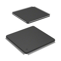
HD6417709SF133B Renesas Electronics America, HD6417709SF133B Datasheet - Page 382

HD6417709SF133B
Manufacturer Part Number
HD6417709SF133B
Description
IC SUPERH MPU ROMLESS 208LQFP
Manufacturer
Renesas Electronics America
Series
SuperH® SH7700r
Datasheet
1.D6417709SBP167BV.pdf
(809 pages)
Specifications of HD6417709SF133B
Core Processor
SH-3
Core Size
32-Bit
Speed
133MHz
Connectivity
EBI/EMI, FIFO, IrDA, SCI, SmartCard
Peripherals
DMA, POR, WDT
Number Of I /o
96
Program Memory Type
ROMless
Ram Size
16K x 8
Voltage - Supply (vcc/vdd)
1.65 V ~ 2.05 V
Data Converters
A/D 8x10b; D/A 2x8b
Oscillator Type
Internal
Operating Temperature
-20°C ~ 75°C
Package / Case
208-LQFP
Lead Free Status / RoHS Status
Contains lead / RoHS non-compliant
Eeprom Size
-
Program Memory Size
-
Available stocks
Company
Part Number
Manufacturer
Quantity
Price
Company:
Part Number:
HD6417709SF133B
Manufacturer:
RENESAS
Quantity:
79
Company:
Part Number:
HD6417709SF133B
Manufacturer:
Renesas Electronics America
Quantity:
10 000
Part Number:
HD6417709SF133B
Manufacturer:
RENESAS/瑞萨
Quantity:
20 000
Part Number:
HD6417709SF133B-V
Manufacturer:
RENESAS/瑞萨
Quantity:
20 000
Part Number:
HD6417709SF133BV
Manufacturer:
RENESAS/瑞萨
Quantity:
20 000
- Current page: 382 of 809
- Download datasheet (5Mb)
11.2.4
DMA channel control registers 0–3 (CHCR0–CHCR3) are 32-bit readable/writable registers that
specify the operation mode, transfer method, etc., for each channel.
Bit 20 is only used in CHCR3; it is not used in CHCR0 to CHCR2. Consequently, writing to this
bit is invalid in CHCR0 to CHCR2; 0 is read if this bit is read. Bit 19 is only used in CHCR2; it is
not used in CHCR0, CHCR1, and CHCR3. Consequently, writing to this bit is invalid in CHCR0,
CHCR1, and CHCR3; 0 is read if this bit is read. Bits 6 and 16 to 18 are only used in CHCR0 and
CHCR1; they are not used in CHCR2 and CHCR3. Consequently, writing to these bits is invalid
in CHCR2 and CHCR3; 0s are read if these bits are read.
These register values are initialized to 0 in a reset. The previous value is retained in standby mode.
Notes: 1. Only 0 can be written to the TE bit after 1 is read.
Rev. 5.00, 09/03, page 336 of 760
Initial value:
Initial value:
Initial value:
2. The DI, RO, RL, AM, AL, and DS bits are not included in some channels.
DMA Channel Control Registers 0–3 (CHCR0–CHCR3)
R/W:
R/W:
R/W:
Bit:
Bit:
Bit:
DM1
R/W
31
15
—
—
R
R
0
0
7
0
(R/W) *
DM0
R/W
DS
14
...
...
...
...
0
6
0
2
SM1
R/W
R/W
TM
21
13
—
R
0
0
5
0
(R/W) *
SM0
R/W
R/W
TS1
20
12
DI
0
0
4
0
2
(R/W) *
RS3
R/W
R/W
TS0
RO
19
11
0
0
3
0
2
(R/W) *
RS2
R/W
R/W
RL
18
10
IE
0
0
2
0
2
(R/W) *
R/(W) *
RS1
R/W
AM
TE
17
0
9
0
1
0
2
1
(R/W) *
RS0
R/W
R/W
DE
AL
16
0
8
0
0
0
2
Related parts for HD6417709SF133B
Image
Part Number
Description
Manufacturer
Datasheet
Request
R

Part Number:
Description:
KIT STARTER FOR M16C/29
Manufacturer:
Renesas Electronics America
Datasheet:

Part Number:
Description:
KIT STARTER FOR R8C/2D
Manufacturer:
Renesas Electronics America
Datasheet:

Part Number:
Description:
R0K33062P STARTER KIT
Manufacturer:
Renesas Electronics America
Datasheet:

Part Number:
Description:
KIT STARTER FOR R8C/23 E8A
Manufacturer:
Renesas Electronics America
Datasheet:

Part Number:
Description:
KIT STARTER FOR R8C/25
Manufacturer:
Renesas Electronics America
Datasheet:

Part Number:
Description:
KIT STARTER H8S2456 SHARPE DSPLY
Manufacturer:
Renesas Electronics America
Datasheet:

Part Number:
Description:
KIT STARTER FOR R8C38C
Manufacturer:
Renesas Electronics America
Datasheet:

Part Number:
Description:
KIT STARTER FOR R8C35C
Manufacturer:
Renesas Electronics America
Datasheet:

Part Number:
Description:
KIT STARTER FOR R8CL3AC+LCD APPS
Manufacturer:
Renesas Electronics America
Datasheet:

Part Number:
Description:
KIT STARTER FOR RX610
Manufacturer:
Renesas Electronics America
Datasheet:

Part Number:
Description:
KIT STARTER FOR R32C/118
Manufacturer:
Renesas Electronics America
Datasheet:

Part Number:
Description:
KIT DEV RSK-R8C/26-29
Manufacturer:
Renesas Electronics America
Datasheet:

Part Number:
Description:
KIT STARTER FOR SH7124
Manufacturer:
Renesas Electronics America
Datasheet:

Part Number:
Description:
KIT STARTER FOR H8SX/1622
Manufacturer:
Renesas Electronics America
Datasheet:

Part Number:
Description:
KIT DEV FOR SH7203
Manufacturer:
Renesas Electronics America
Datasheet:


