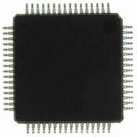
ISP1362BDFA ST-Ericsson Inc, ISP1362BDFA Datasheet - Page 107

ISP1362BDFA
Manufacturer Part Number
ISP1362BDFA
Description
IC USB OTG CONTROLLER 64-LQFP
Manufacturer
ST-Ericsson Inc
Datasheet
1.ISP1362EEUM.pdf
(153 pages)
Specifications of ISP1362BDFA
Controller Type
USB 2.0 Controller
Interface
Parallel/Serial
Voltage - Supply
3 V ~ 3.6 V
Operating Temperature
-40°C ~ 85°C
Mounting Type
Surface Mount
Package / Case
64-LQFP
Lead Free Status / RoHS Status
Lead free / RoHS Compliant
Current - Supply
-
Other names
568-1219
ISP1362BD,151
ISP1362BD-S
ISP1362BD,151
ISP1362BD-S
Available stocks
Company
Part Number
Manufacturer
Quantity
Price
Company:
Part Number:
ISP1362BDFA
Manufacturer:
STE
Quantity:
5
NXP Semiconductors
15. Peripheral Controller registers
Table 108. Peripheral Controller command and register overview
ISP1362_5
Product data sheet
Name
Initialization commands
Write control OUT configuration
Write control IN configuration
Write endpoint n configuration (n = 1
to 14)
Read control OUT configuration
Read control IN configuration
Read endpoint n configuration (n = 1
to 14)
Write or read device address
Write or read Mode register
Write or read hardware configuration
Table 107. HcATLPTDDoneThresholdTimeOut register: bit description
The functions and registers of the Peripheral Controller are accessed using commands,
which consist of a command code followed by optional data bytes (read or write action).
An overview of the available commands and registers is given in
A complete access consists of two phases:
The following applies to a register or buffer memory access in 16-bit bus mode:
Bit
15 to 8
7 to 0
1. Command phase: when address pin A0 = HIGH, the Peripheral Controller interprets
2. Data phase (optional): when address pin A0 = LOW, the Peripheral Controller
•
•
•
the data on the lower byte of the bus (bits D7 to D0) as command code. Commands
without a data phase are immediately executed.
transfers the data on the bus to or from a register or endpoint buffer memory. In case
of multi-byte registers, the least significant byte or word is accessed first.
The upper byte (bits D15 to D8) in the command phase or the undefined byte in the
data phase are ignored.
The access of registers is word-aligned: byte access is not allowed.
If the packet length is odd, the upper byte of the last word in an IN endpoint buffer is
not transmitted to the host. When reading from an OUT endpoint buffer, the upper
byte of the last word must be ignored by the firmware. The packet length is stored in
the first two bytes of the endpoint buffer.
Symbol
-
PTDDoneTimeOut[7:0
]
Destination
DcEndpointConfiguration register
endpoint 0 OUT
DcEndpointConfiguration register
endpoint 0 IN
DcEndpointConfiguration register
endpoint 1 to 14
DcEndpointConfiguration register
endpoint 0 OUT
DcEndpointConfiguration register
endpoint 0 IN
DcEndpointConfiguration register
endpoint 1 to 14
DcAddress register
DcMode register
DcHardwareConfiguration register BA/BB
Rev. 05 — 8 May 2007
Description
reserved
Maximum allowable time in ms for the Host Controller to retry a
transaction with NAK returned.
Code (Hex)
20
21
22 to 2F
30
31
32 to 3F
B6/B7
B8/B9
Single-chip USB OTG Controller
Transaction
write 1 byte
write 1 byte
write 1 byte
read 1 byte
read 1 byte
read 1 byte
write or read 1 byte
write or read 1 byte
write or read 2 bytes
Table
108.
© NXP B.V. 2007. All rights reserved.
ISP1362
[2]
[2]
[2]
[2]
[2]
[2]
[1]
106 of 152
[2]
[2]


