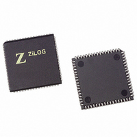
Z16C3516VSG Zilog, Z16C3516VSG Datasheet - Page 27

Z16C3516VSG
Manufacturer Part Number
Z16C3516VSG
Description
IC 16MHZ Z8500 CMOS ISCC 68-PLCC
Manufacturer
Zilog
Series
IUSC™r
Specifications of Z16C3516VSG
Controller Type
Serial Communications Controller (SCC)
Interface
USB
Voltage - Supply
4.75 V ~ 5.25 V
Current - Supply
50mA
Operating Temperature
0°C ~ 70°C
Mounting Type
Surface Mount
Package / Case
68-LCC (J-Lead)
Lead Free Status / RoHS Status
Lead free / RoHS Compliant
Other names
269-4690-5
Z16C3516VSG
Z16C3516VSG
Available stocks
Company
Part Number
Manufacturer
Quantity
Price
Company:
Part Number:
Z16C3516VSG
Manufacturer:
INTEL
Quantity:
6 219
- Current page: 27 of 268
- Download datasheet (3Mb)
UM011001-0601
In the NRZI mode, the DPLL clock must be 32 times the
data rate. In this mode, the transmit and receive clock out-
puts of the DPLL are identical, and the clocks are phased
so that the receiver samples the data in the middle of the
bit cell. In NRZI mode, the DPLL does not require a transi-
tion in every bit cell, so this mode is useful for recovering
the clocking information from NRZ and NRZI data streams.
In the FM mode, the DPLL clock must be 16 times the data
rate. In this mode the transmit clock output of the DPLL
lags the receive clock outputs by 90 degrees to make the
transmit and receive bit cell boundaries the same, be-
cause the receiver must sample FM data at one-quarter
and three-quarters bit time.
Ordinarily, a bit cell boundary will occur between count 15
and count 16, and the DPLL output will cause the data to
be sampled in the middle of the bit cell. However, four dif-
ferent situations may happen:
The DPLL actually allows the transition marking a bit cell
boundary to occur anywhere during the second half of
count 15 or the first half of count 16 without making a cor-
rection to its count cycle.
If the transition marking a bit cell boundary occurs between
the middle of count 16 and count 31, the DPLL is sampling
the data too early in the bit cell. In response to this, the
DPLL extends its count by one during the next 0 to 31
counting cycle, which effectively moves the edge of the
clock that samples the receive data closer to the center of
the bit cell.
If the transition occurs between count 0 and the middle of
count 15, the output of the DPLL is sampling the data too
Connection
DPLL Out
Bit Cell
Count
16
No Change
17
18 19 20
21 22 23 24 25 26 27 28 29 30 31
Add One Count
Figure 3-5. DPLL in NRZI Mode
3.5.1 DPLL Operation in the NRZI Mode
To operate in NRZI mode, the DPLL must be supplied with
a clock that is 32 times the data rate. The DPLL uses this
clock, along with the receive data, to construct receive and
transmit clock outputs that are phased to properly receive
and transmit data.
To do this, the DPLL divides each bit cell into four regions,
and makes an adjustment to the count cycle of the 5-bit
counter dependent upon in which region a transition on the
receive data input occurred. This is shown in Figure 3-5.
late in the bit cell. To correct this, the DPLL shortens its
count by one during the next 0 to 31 counting cycle, which
effectively moves the edge of the clock that samples the
receive data closer to the center of the bit cell.
If the DPLL does not see any transition during a counting cy-
cle, no adjustment is made in the following counting cycle.
If an adjustment to the counting cycle is necessary, the
DPLL modifies count 5, either deleting it or doubling it.
Thus, only the LOW time of the DPLL output will be length-
ened or shortened.
While the DPLL is in search mode, the counter remains at
count 16 where the DPLL outputs are both HIGH. The
missing clock latches in the DPLL which may be accessed
in RR10. They are not used in NRZI mode. An example of
the DPLL in operation is shown in Figure 3-6.
0
1
ISCC™ DMA and Ancillary Support Circuitry
2 3 4 5
Subtract One Count
6
Z16C35ISCC™ User’s Manual
7 8 9
10
11
No Change
12 13 14
15
3-7
3
Related parts for Z16C3516VSG
Image
Part Number
Description
Manufacturer
Datasheet
Request
R

Part Number:
Description:
CMOS ISCC INTEGRATED SERIAL COMMUNICATIONS CONTROLLER
Manufacturer:
ZILOG [Zilog, Inc.]
Datasheet:

Part Number:
Description:
Communication Controllers, ZILOG INTELLIGENT PERIPHERAL CONTROLLER (ZIP)
Manufacturer:
Zilog, Inc.
Datasheet:

Part Number:
Description:
KIT DEV FOR Z8 ENCORE 16K TO 64K
Manufacturer:
Zilog
Datasheet:

Part Number:
Description:
KIT DEV Z8 ENCORE XP 28-PIN
Manufacturer:
Zilog
Datasheet:

Part Number:
Description:
DEV KIT FOR Z8 ENCORE 8K/4K
Manufacturer:
Zilog
Datasheet:

Part Number:
Description:
KIT DEV Z8 ENCORE XP 28-PIN
Manufacturer:
Zilog
Datasheet:

Part Number:
Description:
DEV KIT FOR Z8 ENCORE 4K TO 8K
Manufacturer:
Zilog
Datasheet:

Part Number:
Description:
CMOS Z8 microcontroller. ROM 16 Kbytes, RAM 256 bytes, speed 16 MHz, 32 lines I/O, 3.0V to 5.5V
Manufacturer:
Zilog, Inc.
Datasheet:

Part Number:
Description:
Low-cost microcontroller. 512 bytes ROM, 61 bytes RAM, 8 MHz
Manufacturer:
Zilog, Inc.
Datasheet:

Part Number:
Description:
Z8 4K OTP Microcontroller
Manufacturer:
Zilog, Inc.
Datasheet:

Part Number:
Description:
CMOS SUPER8 ROMLESS MCU
Manufacturer:
Zilog, Inc.
Datasheet:

Part Number:
Description:
SL1866 CMOSZ8 OTP Microcontroller
Manufacturer:
Zilog, Inc.
Datasheet:

Part Number:
Description:
SL1866 CMOSZ8 OTP Microcontroller
Manufacturer:
Zilog, Inc.
Datasheet:

Part Number:
Description:
OTP (KB) = 1, RAM = 125, Speed = 12, I/O = 14, 8-bit Timers = 2, Comm Interfaces Other Features = Por, LV Protect, Voltage = 4.5-5.5V
Manufacturer:
Zilog, Inc.
Datasheet:


