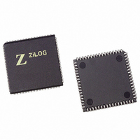
Z16C3516VSG Zilog, Z16C3516VSG Datasheet - Page 76

Z16C3516VSG
Manufacturer Part Number
Z16C3516VSG
Description
IC 16MHZ Z8500 CMOS ISCC 68-PLCC
Manufacturer
Zilog
Series
IUSC™r
Specifications of Z16C3516VSG
Controller Type
Serial Communications Controller (SCC)
Interface
USB
Voltage - Supply
4.75 V ~ 5.25 V
Current - Supply
50mA
Operating Temperature
0°C ~ 70°C
Mounting Type
Surface Mount
Package / Case
68-LCC (J-Lead)
Lead Free Status / RoHS Status
Lead free / RoHS Compliant
Other names
269-4690-5
Z16C3516VSG
Z16C3516VSG
Available stocks
Company
Part Number
Manufacturer
Quantity
Price
Company:
Part Number:
Z16C3516VSG
Manufacturer:
INTEL
Quantity:
6 219
- Current page: 76 of 268
- Download datasheet (3Mb)
Z16C35ISCC™ User’s Manual
Register Descriptions
5.4 WRITE REGISTERS (Continued)
In synchronous modes, the ISCC uses this bit, along with
the Go Active On Poll bit, to synchronize the transmitter to
the receiver. The receiver should not be enabled until after
this mode is selected. The TxD pin is held marking when
this mode is selected unless a break condition is pro-
grammed. The receiver waits for a sync character to be re-
ceived and then enables the transmitter on a character
boundary. The break condition, if programmed, is re-
moved. This mode works properly with sync characters of
6, 8, or 16 bits. This bit is ignored in Asynchronous mode
and is reset by a channel or hardware reset.
Bit 0 is the 6-Bit//8-Bit SYNC select bit
This bit is used to select a special case of synchronous
modes. If this bit is set to “1” in Monosync mode, the
Bit 7 is the RTxC-XTAL//NO XTAL select bit
This bit controls the type of input signal the ISCC expects
to see on the /RTxC pin. If this bit is set to “0,” the ISCC
expects a TTL-compatible signal as an input to this pin. If
this bit is set to “1,” the ISCC connects a high-gain amplifi-
er between the /RTxC and /SYNC pins in expectation of a
quartz crystal being placed across the pins.
The output of this oscillator is available for use as a clock-
ing source. In this mode of operation, the /SYNC pin is un-
available for other use. The /SYNC signal is forced to “0”
internally. A hardware reset forces /NO XTAL. (At least 20
5-16
Write Register 11
D7
D6
0
0
1
1
D5 D4 D3 D2 D1 D0
0
1
0
1
0
0
1
1
Receive Clock = /RTxC Pin
Receive Clock = /TRxC Pin
Receive Clock = BR Generator Output
Receive Clock = DPLL Output
0
1
0
1
Figure 5-13. Write Register 11
Transmit Clock = /RTxC Pin
Transmit Clock = /TRxC Pin
Transmit Clock = BR Generator Output
Transmit Clock = DPLL Output
0
0
1
1
P R E L I M I N A R Y
0
1
0
1
/TRxC Out = Xtal Output
/TRxC Out = Transmit Clock
/TRxC Out = BR Generator Output
/TRxC Out = DPLL Output
TRxC O/I
/RTxC Xtal/No Xtal
receiver and transmitter sync characters are six bits long
instead of the usual eight. If this bit is set to “1” in Bisync
mode, the received sync will be 12 bits and the transmitter
sync character will remain 16 bits long. This bit is ignored
in SDLC and Asynchronous modes, but still has effect in
the special external sync modes. This bit is reset by a
channel or hardware reset.
5.4.12 Write Register 11 (Clock Mode Control)
WR11 is the Clock Mode Control register. The bits in this
register control the sources of both the receive and trans-
mit clocks, the type of signal on the /SYNC and /RTxC
pins, and the direction of the /TRxC pin. Bit positions for
WR11 are shown in Figure 5-13.
ms should be allowed after this bit is set to 1, to allow the
oscillator to stabilize.)
Bits 6 and 5 are the Receiver Clock select bits 1 and 0
These bits determine the source of the receive clock as
shown in Table 5-9. They do not interfere with any of the
modes of operation in the SCC cell, but simply control a
multiplexer just before the internal receive clock input. A
hardware reset forces the receive clock to come from the
/RTxC pin.
UM011001-0601
Related parts for Z16C3516VSG
Image
Part Number
Description
Manufacturer
Datasheet
Request
R

Part Number:
Description:
CMOS ISCC INTEGRATED SERIAL COMMUNICATIONS CONTROLLER
Manufacturer:
ZILOG [Zilog, Inc.]
Datasheet:

Part Number:
Description:
Communication Controllers, ZILOG INTELLIGENT PERIPHERAL CONTROLLER (ZIP)
Manufacturer:
Zilog, Inc.
Datasheet:

Part Number:
Description:
KIT DEV FOR Z8 ENCORE 16K TO 64K
Manufacturer:
Zilog
Datasheet:

Part Number:
Description:
KIT DEV Z8 ENCORE XP 28-PIN
Manufacturer:
Zilog
Datasheet:

Part Number:
Description:
DEV KIT FOR Z8 ENCORE 8K/4K
Manufacturer:
Zilog
Datasheet:

Part Number:
Description:
KIT DEV Z8 ENCORE XP 28-PIN
Manufacturer:
Zilog
Datasheet:

Part Number:
Description:
DEV KIT FOR Z8 ENCORE 4K TO 8K
Manufacturer:
Zilog
Datasheet:

Part Number:
Description:
CMOS Z8 microcontroller. ROM 16 Kbytes, RAM 256 bytes, speed 16 MHz, 32 lines I/O, 3.0V to 5.5V
Manufacturer:
Zilog, Inc.
Datasheet:

Part Number:
Description:
Low-cost microcontroller. 512 bytes ROM, 61 bytes RAM, 8 MHz
Manufacturer:
Zilog, Inc.
Datasheet:

Part Number:
Description:
Z8 4K OTP Microcontroller
Manufacturer:
Zilog, Inc.
Datasheet:

Part Number:
Description:
CMOS SUPER8 ROMLESS MCU
Manufacturer:
Zilog, Inc.
Datasheet:

Part Number:
Description:
SL1866 CMOSZ8 OTP Microcontroller
Manufacturer:
Zilog, Inc.
Datasheet:

Part Number:
Description:
SL1866 CMOSZ8 OTP Microcontroller
Manufacturer:
Zilog, Inc.
Datasheet:

Part Number:
Description:
OTP (KB) = 1, RAM = 125, Speed = 12, I/O = 14, 8-bit Timers = 2, Comm Interfaces Other Features = Por, LV Protect, Voltage = 4.5-5.5V
Manufacturer:
Zilog, Inc.
Datasheet:


