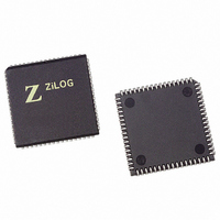
Z16C3516VSG Zilog, Z16C3516VSG Datasheet - Page 89

Z16C3516VSG
Manufacturer Part Number
Z16C3516VSG
Description
IC 16MHZ Z8500 CMOS ISCC 68-PLCC
Manufacturer
Zilog
Series
IUSC™r
Specifications of Z16C3516VSG
Controller Type
Serial Communications Controller (SCC)
Interface
USB
Voltage - Supply
4.75 V ~ 5.25 V
Current - Supply
50mA
Operating Temperature
0°C ~ 70°C
Mounting Type
Surface Mount
Package / Case
68-LCC (J-Lead)
Lead Free Status / RoHS Status
Lead free / RoHS Compliant
Other names
269-4690-5
Z16C3516VSG
Z16C3516VSG
Available stocks
Company
Part Number
Manufacturer
Quantity
Price
Company:
Part Number:
Z16C3516VSG
Manufacturer:
INTEL
Quantity:
6 219
- Current page: 89 of 268
- Download datasheet (3Mb)
UM011001-0601
5.6.7 DMA Enable Register
This register controls the enabling of the DMA channels
and contains the enables for the DMA Abort Interrupt con-
ditions. The bit positions for this register are shown in Fig-
ure 5-32.
Bit 7, when set to 1, enables the Receive A DMA.
Bit 6, when set to 1, enables the Transmit A DMA.
Bit 5, when set to 1, enables the Receive B DMA.
Bit 4, when set to 1, enables the Transmit B DMA.
Bit 3, when set to 1, enables the interrupt in the Receive A
DMA Channel that is generated when a DMA operation in
this channel is aborted.
Bit 2, when set to 1, enables the interrupt in the Transmit
A DMA Channel that is generated when a DMA operation
in this channel is aborted.
Bit 1, when set to 1, enables the interrupt in the Receive B
DMA Channel that is generated when a DMA operation in
this channel is aborted.
Bit 0, when set to 1, enables the interrupt in the Transmit
B DMA Channel that is generated when a DMA operation
in this channel is aborted.
Address: 00100
D7
D6
D5 D4 D3 D2 D1 D0
Figure 5-32. DMA Enable Register
Rx B DMA Abort Enable
Rx A DMA Abort Enable
Tx B DMA Abort Enable
Tx A DMA Abort Enable
Tx B DMA Enable
Rx B DMA Enable
Tx A DMA Enable
Rx A DMA Enable
P R E L I M I N A R Y
5.6.8 DMA Control Register
This register controls DMA priorities, requests, and ad-
dress generation. The bit positions for this register are
shown in Figure 5-33.
Bit 7, when set to 1, enables a bus request per channel. This
means that if more than one DMA request is pending, after
the completion of a DMA transfer from one DMA channel,
the bus will be relinquished and subsequently requested for
the other channel DMA requests. If this bit is cleared (0), the
DMA will hold the bus until there are no DMA requests
pending, thus multiple channels may make DMA transfers
without separate, intervening bus acquisitions.
Bit 6 is reserved and should be programmed zero.
Bits 5 and 4 control the DMA priority according to Table 5-
15. If DMA requests arise simultaneously, the channel
which is serviced first is the one with the highest priority as
programmed. Note that the interrupt priorities are not af-
fected by this programming and remain fixed in the order
Rx A DMA (highest), Tx A DMA, Rx B DMA, Tx B DMA
(lowest).
Address: 00101
D7
D6
D5 D4 D3 D2 D1 D0
0
0
1
1
Figure 5-33. DMA Control Register
0
1
0
1
DMA Priority
Rx A/Tx A/Rx B/Tx B
Rx B/Tx B/Rx A/Tx A
Rx A/Rx B/Tx A/Tx B
Rx B/Rx A/Tx B/Tx A
Z16C35ISCC™ User’s Manual
Rx B DMA Address Inc/Dec
Rx A DMA Address Inc/Dec
Tx B DMA Address Inc/Dec
Tx A DMA Address Inc/Dec
Reserved
Bus Request per Channel
Register Descriptions
5-29
5
Related parts for Z16C3516VSG
Image
Part Number
Description
Manufacturer
Datasheet
Request
R

Part Number:
Description:
CMOS ISCC INTEGRATED SERIAL COMMUNICATIONS CONTROLLER
Manufacturer:
ZILOG [Zilog, Inc.]
Datasheet:

Part Number:
Description:
Communication Controllers, ZILOG INTELLIGENT PERIPHERAL CONTROLLER (ZIP)
Manufacturer:
Zilog, Inc.
Datasheet:

Part Number:
Description:
KIT DEV FOR Z8 ENCORE 16K TO 64K
Manufacturer:
Zilog
Datasheet:

Part Number:
Description:
KIT DEV Z8 ENCORE XP 28-PIN
Manufacturer:
Zilog
Datasheet:

Part Number:
Description:
DEV KIT FOR Z8 ENCORE 8K/4K
Manufacturer:
Zilog
Datasheet:

Part Number:
Description:
KIT DEV Z8 ENCORE XP 28-PIN
Manufacturer:
Zilog
Datasheet:

Part Number:
Description:
DEV KIT FOR Z8 ENCORE 4K TO 8K
Manufacturer:
Zilog
Datasheet:

Part Number:
Description:
CMOS Z8 microcontroller. ROM 16 Kbytes, RAM 256 bytes, speed 16 MHz, 32 lines I/O, 3.0V to 5.5V
Manufacturer:
Zilog, Inc.
Datasheet:

Part Number:
Description:
Low-cost microcontroller. 512 bytes ROM, 61 bytes RAM, 8 MHz
Manufacturer:
Zilog, Inc.
Datasheet:

Part Number:
Description:
Z8 4K OTP Microcontroller
Manufacturer:
Zilog, Inc.
Datasheet:

Part Number:
Description:
CMOS SUPER8 ROMLESS MCU
Manufacturer:
Zilog, Inc.
Datasheet:

Part Number:
Description:
SL1866 CMOSZ8 OTP Microcontroller
Manufacturer:
Zilog, Inc.
Datasheet:

Part Number:
Description:
SL1866 CMOSZ8 OTP Microcontroller
Manufacturer:
Zilog, Inc.
Datasheet:

Part Number:
Description:
OTP (KB) = 1, RAM = 125, Speed = 12, I/O = 14, 8-bit Timers = 2, Comm Interfaces Other Features = Por, LV Protect, Voltage = 4.5-5.5V
Manufacturer:
Zilog, Inc.
Datasheet:


