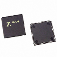
Z16C3516VSG Zilog, Z16C3516VSG Datasheet - Page 86

Z16C3516VSG
Manufacturer Part Number
Z16C3516VSG
Description
IC 16MHZ Z8500 CMOS ISCC 68-PLCC
Manufacturer
Zilog
Series
IUSC™r
Specifications of Z16C3516VSG
Controller Type
Serial Communications Controller (SCC)
Interface
USB
Voltage - Supply
4.75 V ~ 5.25 V
Current - Supply
50mA
Operating Temperature
0°C ~ 70°C
Mounting Type
Surface Mount
Package / Case
68-LCC (J-Lead)
Lead Free Status / RoHS Status
Lead free / RoHS Compliant
Other names
269-4690-5
Z16C3516VSG
Z16C3516VSG
Available stocks
Company
Part Number
Manufacturer
Quantity
Price
Company:
Part Number:
Z16C3516VSG
Manufacturer:
INTEL
Quantity:
6 219
- Current page: 86 of 268
- Download datasheet (3Mb)
Z16C35ISCC™ User’s Manual
Register Descriptions
5.6 DMA CELL REGISTER DESCRIPTIONS (Continued)
Bit combination 110 is the command to enable the Trans-
mitter A channel DMA. The DMA operation is not triggered
by this command.
Bit combination 111 is the command to enable the Receiv-
er B channel DMA. The DMA operation is not triggered by
this command.
Bits 4 through 0 comprise the pointer to the internal regis-
ters. This pointer is used in the non-multiplexed bus modes
to access the DMA cell internal registers. After reset, the
internal pointer points to the Channel Command/Address
Register. Access to other registers is accomplished by first
writing the address of the desired register to this field. The
next access to the DMA cell will be to the register so ad-
dressed; this access may be a read or a write. After this
second access (the access to the desired register), the in-
ternal pointer latch is cleared and the pointer again points
to the Channel Command/Address Register.
5.6.2 DMA Status Register
This register is a read only register and is at the same ad-
dress as the Channel Command/Address Register. The in-
dividual bits indicate abort and terminal count of each of
the four DMA channels. Figure 5-27 shows the bit posi-
tions for the DMA Status Register. The status in this regis-
ter is automatically cleared after a read.
Bit 7, when set, indicates that the Receiver A DMA has
reached terminal count.
Bit 6, when set, indicates that the Transmitter A DMA has
reached terminal count.
5-26
Address: 00000 (Read)
D7
D6
D5 D4 D3 D2 D1 D0
Figure 5-27. DMA Status Register
Tx B DMA Abort
Rx B DMA Abort
Tx A DMA Abort
Rx A DMA Abort
Tx B DMA Terminal Count
Rx B DMA Terminal Count
Tx A DMA Terminal Count
Rx A DMA Terminal Count
P R E L I M I N A R Y
Bit 5, when set, indicates that the Receiver B DMA has
reached terminal count.
Bit 4, when set, indicates that the Transmitter B DMA has
reached terminal count.
Bit 3, when set, indicates that the Receiver A DMA opera-
tion has been aborted.
Bit 2, when set, indicates that the Transmitter A DMA op-
eration has been aborted.
Bit 1, when set, indicates that the Receiver B DMA opera-
tion has been aborted.
Bit 0, when set, indicates that the Transmitter B DMA op-
eration has been aborted.
5.6.3 Interrupt Control Register
The Interrupt Control Register is used to enable the inter-
rupts from the individual sources, and select the interrupt
vector options. This register is read/write. The bit positions
are shown in Figure 5-28.
Bit 7 is the Master Interrupt Enable (MIE). When this bit is
cleared, all interrupts from the DMA cell are disabled even
though the individual enable bits are set. This bit must be
set for any DMA interrupt source to cause an interrupt.
Bit 6 is the disable lower chain control bit (DLC). If this bit
is set, the external lower chain of the daisy chained inter-
rupt structure is disabled; IEO will not become active.
Address: 00001
D7
D6
Figure 5-28. Interrupt Control Register
D5 D4 D3 D2 D1 D0
Tx A DMA Interrupt Enable
Tx B DMA Interrupt Enable
Rx B DMA Interrupt Enable
Rx A DMA Interrupt Enable
VIS
NV
DLC
MIE
UM011001-0601
Related parts for Z16C3516VSG
Image
Part Number
Description
Manufacturer
Datasheet
Request
R

Part Number:
Description:
CMOS ISCC INTEGRATED SERIAL COMMUNICATIONS CONTROLLER
Manufacturer:
ZILOG [Zilog, Inc.]
Datasheet:

Part Number:
Description:
Communication Controllers, ZILOG INTELLIGENT PERIPHERAL CONTROLLER (ZIP)
Manufacturer:
Zilog, Inc.
Datasheet:

Part Number:
Description:
KIT DEV FOR Z8 ENCORE 16K TO 64K
Manufacturer:
Zilog
Datasheet:

Part Number:
Description:
KIT DEV Z8 ENCORE XP 28-PIN
Manufacturer:
Zilog
Datasheet:

Part Number:
Description:
DEV KIT FOR Z8 ENCORE 8K/4K
Manufacturer:
Zilog
Datasheet:

Part Number:
Description:
KIT DEV Z8 ENCORE XP 28-PIN
Manufacturer:
Zilog
Datasheet:

Part Number:
Description:
DEV KIT FOR Z8 ENCORE 4K TO 8K
Manufacturer:
Zilog
Datasheet:

Part Number:
Description:
CMOS Z8 microcontroller. ROM 16 Kbytes, RAM 256 bytes, speed 16 MHz, 32 lines I/O, 3.0V to 5.5V
Manufacturer:
Zilog, Inc.
Datasheet:

Part Number:
Description:
Low-cost microcontroller. 512 bytes ROM, 61 bytes RAM, 8 MHz
Manufacturer:
Zilog, Inc.
Datasheet:

Part Number:
Description:
Z8 4K OTP Microcontroller
Manufacturer:
Zilog, Inc.
Datasheet:

Part Number:
Description:
CMOS SUPER8 ROMLESS MCU
Manufacturer:
Zilog, Inc.
Datasheet:

Part Number:
Description:
SL1866 CMOSZ8 OTP Microcontroller
Manufacturer:
Zilog, Inc.
Datasheet:

Part Number:
Description:
SL1866 CMOSZ8 OTP Microcontroller
Manufacturer:
Zilog, Inc.
Datasheet:

Part Number:
Description:
OTP (KB) = 1, RAM = 125, Speed = 12, I/O = 14, 8-bit Timers = 2, Comm Interfaces Other Features = Por, LV Protect, Voltage = 4.5-5.5V
Manufacturer:
Zilog, Inc.
Datasheet:


