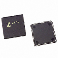
Z16C3516VSG Zilog, Z16C3516VSG Datasheet - Page 85

Z16C3516VSG
Manufacturer Part Number
Z16C3516VSG
Description
IC 16MHZ Z8500 CMOS ISCC 68-PLCC
Manufacturer
Zilog
Series
IUSC™r
Specifications of Z16C3516VSG
Controller Type
Serial Communications Controller (SCC)
Interface
USB
Voltage - Supply
4.75 V ~ 5.25 V
Current - Supply
50mA
Operating Temperature
0°C ~ 70°C
Mounting Type
Surface Mount
Package / Case
68-LCC (J-Lead)
Lead Free Status / RoHS Status
Lead free / RoHS Compliant
Other names
269-4690-5
Z16C3516VSG
Z16C3516VSG
Available stocks
Company
Part Number
Manufacturer
Quantity
Price
Company:
Part Number:
Z16C3516VSG
Manufacturer:
INTEL
Quantity:
6 219
- Current page: 85 of 268
- Download datasheet (3Mb)
UM011001-0601
5.5.8 Read Register 13
RR13 returns the value stored in WR13, the upper byte of
the time constant for the baud rate generator. Figure 5-24
shows the bit positions for RR13.
5.6 DMA CELL REGISTER DESCRIPTIONS
5.6.1 Channel Command/Address Register
This register is a write only register and is at the same ad-
dress as the DMA Status Register. Figure 5-26 shows the
bit positions for this register.
Bits 7 through 5 are encoded with the commands for the
DMA as shown below:
Bit combination 000 is a Null command and has no affect
on the DMA.
Bit combination 001 is reserved
Bit combination 010 is the DMA Reset Highest IUS com-
mand. This command resets only the highest priority IUS
bit that is set in the DMA cell and occurs independent of
the state of the IEI for the ISCC.
Bit combination 011 is the Reset command and is used to
reset the DMA cell. All of the DMA channels are reset. The
DMA channels remain reset until enabled.
Bit combination 100 is the command to enable the Trans-
mitter B channel DMA. The DMA operation is not triggered
by this command.
Read Register 13
D7
D6
D5 D4 D3 D2 D1 D0
Figure 5-24. Read Register 13
TC8
TC9
TC10
TC11
TC12
TC13
TC14
TC15
Upper
Byte of
Time
Constant
P R E L I M I N A R Y
5.5.9 Read Register 15
RR15 reflects the value stored in WR15, the External/Sta-
tus IE bits. The two unused bits are always returned as
“0s”. Figure 5-25 shows the bits positions for RR15.
Bit combination 101 is the command to enable the Receiv-
er B channel DMA. The DMA operation is not triggered by
this command.
Read Register 15
D7
Figure 5-26. Channel Command/Address Register
Address: 00000 (Write)
D7
0
0
0
0
1
1
1
1
D6
D6
0
0
1
1
0
0
1
1
D5 D4 D3 D2 D1 D0
D5 D4 D3 D2 D1 D0
Figure 5-25. Read Register 15
0
1
0
1
0
1
0
1
DMA Commands
Null Command
Reserved
Reset Highest IUS
DMA Reset
Enable Tx B DMA
Enable Rx B DMA
Enable Tx A DMA
Enable Rx A DMA
Z16C35ISCC™ User’s Manual
Register Descriptions
0
Zero Count IE
0
DCD IE
Sync/Hunt IE
CTS IE
Tx Underrun/EOM IE
Break/Abort IE
Address 0
Address 1
Address 2
Address 3
Address 4
5-25
5
Related parts for Z16C3516VSG
Image
Part Number
Description
Manufacturer
Datasheet
Request
R

Part Number:
Description:
CMOS ISCC INTEGRATED SERIAL COMMUNICATIONS CONTROLLER
Manufacturer:
ZILOG [Zilog, Inc.]
Datasheet:

Part Number:
Description:
Communication Controllers, ZILOG INTELLIGENT PERIPHERAL CONTROLLER (ZIP)
Manufacturer:
Zilog, Inc.
Datasheet:

Part Number:
Description:
KIT DEV FOR Z8 ENCORE 16K TO 64K
Manufacturer:
Zilog
Datasheet:

Part Number:
Description:
KIT DEV Z8 ENCORE XP 28-PIN
Manufacturer:
Zilog
Datasheet:

Part Number:
Description:
DEV KIT FOR Z8 ENCORE 8K/4K
Manufacturer:
Zilog
Datasheet:

Part Number:
Description:
KIT DEV Z8 ENCORE XP 28-PIN
Manufacturer:
Zilog
Datasheet:

Part Number:
Description:
DEV KIT FOR Z8 ENCORE 4K TO 8K
Manufacturer:
Zilog
Datasheet:

Part Number:
Description:
CMOS Z8 microcontroller. ROM 16 Kbytes, RAM 256 bytes, speed 16 MHz, 32 lines I/O, 3.0V to 5.5V
Manufacturer:
Zilog, Inc.
Datasheet:

Part Number:
Description:
Low-cost microcontroller. 512 bytes ROM, 61 bytes RAM, 8 MHz
Manufacturer:
Zilog, Inc.
Datasheet:

Part Number:
Description:
Z8 4K OTP Microcontroller
Manufacturer:
Zilog, Inc.
Datasheet:

Part Number:
Description:
CMOS SUPER8 ROMLESS MCU
Manufacturer:
Zilog, Inc.
Datasheet:

Part Number:
Description:
SL1866 CMOSZ8 OTP Microcontroller
Manufacturer:
Zilog, Inc.
Datasheet:

Part Number:
Description:
SL1866 CMOSZ8 OTP Microcontroller
Manufacturer:
Zilog, Inc.
Datasheet:

Part Number:
Description:
OTP (KB) = 1, RAM = 125, Speed = 12, I/O = 14, 8-bit Timers = 2, Comm Interfaces Other Features = Por, LV Protect, Voltage = 4.5-5.5V
Manufacturer:
Zilog, Inc.
Datasheet:


