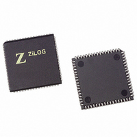
Z16C3516VSG Zilog, Z16C3516VSG Datasheet - Page 36

Z16C3516VSG
Manufacturer Part Number
Z16C3516VSG
Description
IC 16MHZ Z8500 CMOS ISCC 68-PLCC
Manufacturer
Zilog
Series
IUSC™r
Specifications of Z16C3516VSG
Controller Type
Serial Communications Controller (SCC)
Interface
USB
Voltage - Supply
4.75 V ~ 5.25 V
Current - Supply
50mA
Operating Temperature
0°C ~ 70°C
Mounting Type
Surface Mount
Package / Case
68-LCC (J-Lead)
Lead Free Status / RoHS Status
Lead free / RoHS Compliant
Other names
269-4690-5
Z16C3516VSG
Z16C3516VSG
Available stocks
Company
Part Number
Manufacturer
Quantity
Price
Company:
Part Number:
Z16C3516VSG
Manufacturer:
INTEL
Quantity:
6 219
- Current page: 36 of 268
- Download datasheet (3Mb)
Z16C35ISCC™ User’s Manual
Data Communication Modes
4.1 INTRODUCTION (Continued)
If asynchronous data is processed, WR6 and WR7 are not
used and the Transmit Shift register is formatted with start
and stop bits shifted out to the transmit multiplexer at the
selected
SDLC/HDLC) is shifted to the CRC generator as well as to
the transmit multiplexer.
SDLC/HDLC data is shifted to the CRC Generator and out
through the zero insertion logic (which is disabled while the
flags are being sent). A “0” is inserted in all address, con-
trol, information, and frame check fields following five con-
tiguous “1s” in the data stream. The result of the CRC gen-
erator for SDLC data is also routed through the zero
insertion logic and then to the transmit multiplexer.
4-2
Internal Data Bus
clock
WR7 Sync
Register
Transmit
20-Bit
CRC SDLC
rate.
Zero Insert
Generator
(5-Bits)
CRC
Synchronous
SDLC
WR6 Sync
Register
Register
SYNC
Shift
Figure 4-1. Transmitter Block Diagram
data
ASYNC
WR5 Transmit
(except
2-Bit Delay
Transmit
Transmit
Start
MUX &
Data
Clock
Bit
4.1.2 General Description of the Receiver
The receiver has a three deep, 8-bit Data FIFO (paired
with a three deep Error FIFO), and an 8-bit shift register.
The receiver block diagram is shown in Figure 4-2. This
arrangement creates a three-character delay time, which
allows the CPU time to service an interrupt at the
beginning of a block of high-speed data. With each
Receive Data FIFO, the Error FIFO stores parity and
framing errors and other types of status information. The
Error FIFO is readable in Read Register 1.
Internal
Encode
NRZI
TxD
Final Tx
MUX
To Other
Channel
RxD Delayed
One Bit
RxD
TxD
UM011001-0601
Related parts for Z16C3516VSG
Image
Part Number
Description
Manufacturer
Datasheet
Request
R

Part Number:
Description:
CMOS ISCC INTEGRATED SERIAL COMMUNICATIONS CONTROLLER
Manufacturer:
ZILOG [Zilog, Inc.]
Datasheet:

Part Number:
Description:
Communication Controllers, ZILOG INTELLIGENT PERIPHERAL CONTROLLER (ZIP)
Manufacturer:
Zilog, Inc.
Datasheet:

Part Number:
Description:
KIT DEV FOR Z8 ENCORE 16K TO 64K
Manufacturer:
Zilog
Datasheet:

Part Number:
Description:
KIT DEV Z8 ENCORE XP 28-PIN
Manufacturer:
Zilog
Datasheet:

Part Number:
Description:
DEV KIT FOR Z8 ENCORE 8K/4K
Manufacturer:
Zilog
Datasheet:

Part Number:
Description:
KIT DEV Z8 ENCORE XP 28-PIN
Manufacturer:
Zilog
Datasheet:

Part Number:
Description:
DEV KIT FOR Z8 ENCORE 4K TO 8K
Manufacturer:
Zilog
Datasheet:

Part Number:
Description:
CMOS Z8 microcontroller. ROM 16 Kbytes, RAM 256 bytes, speed 16 MHz, 32 lines I/O, 3.0V to 5.5V
Manufacturer:
Zilog, Inc.
Datasheet:

Part Number:
Description:
Low-cost microcontroller. 512 bytes ROM, 61 bytes RAM, 8 MHz
Manufacturer:
Zilog, Inc.
Datasheet:

Part Number:
Description:
Z8 4K OTP Microcontroller
Manufacturer:
Zilog, Inc.
Datasheet:

Part Number:
Description:
CMOS SUPER8 ROMLESS MCU
Manufacturer:
Zilog, Inc.
Datasheet:

Part Number:
Description:
SL1866 CMOSZ8 OTP Microcontroller
Manufacturer:
Zilog, Inc.
Datasheet:

Part Number:
Description:
SL1866 CMOSZ8 OTP Microcontroller
Manufacturer:
Zilog, Inc.
Datasheet:

Part Number:
Description:
OTP (KB) = 1, RAM = 125, Speed = 12, I/O = 14, 8-bit Timers = 2, Comm Interfaces Other Features = Por, LV Protect, Voltage = 4.5-5.5V
Manufacturer:
Zilog, Inc.
Datasheet:


