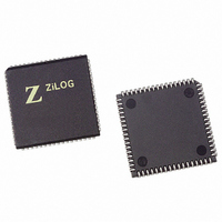
Z16C3516VSG Zilog, Z16C3516VSG Datasheet - Page 90

Z16C3516VSG
Manufacturer Part Number
Z16C3516VSG
Description
IC 16MHZ Z8500 CMOS ISCC 68-PLCC
Manufacturer
Zilog
Series
IUSC™r
Specifications of Z16C3516VSG
Controller Type
Serial Communications Controller (SCC)
Interface
USB
Voltage - Supply
4.75 V ~ 5.25 V
Current - Supply
50mA
Operating Temperature
0°C ~ 70°C
Mounting Type
Surface Mount
Package / Case
68-LCC (J-Lead)
Lead Free Status / RoHS Status
Lead free / RoHS Compliant
Other names
269-4690-5
Z16C3516VSG
Z16C3516VSG
Available stocks
Company
Part Number
Manufacturer
Quantity
Price
Company:
Part Number:
Z16C3516VSG
Manufacturer:
INTEL
Quantity:
6 219
- Current page: 90 of 268
- Download datasheet (3Mb)
Z16C35ISCC™ User’s Manual
Register Descriptions
5.6 DMA CELL REGISTER DESCRIPTIONS (Continued)
Bit 3 selects if the DMA address for the Receive A DMA is
to be incremented or decremented after each DMA byte
transfer. Programming this bit to a 1 causes the address to
increment; programming this bit to a 0 causes the address
to decrement.
Bit 2 selects if the DMA address for the Transmit A DMA is
to be incremented or decremented after each DMA byte
transfer. Its operation is identical to bit 3.
5-30
D5
0
0
1
1
Address: 01000 (Low Byte)
Address: 01100 (Low Byte)
D7
D7
D6
D6
Table 5-15. DMA Priority
D5 D4 D3 D2 D1 D0
D5 D4 D3 D2 D1 D0
D4
0
1
0
1
DMA Priority
Rx A/Tx A/Rx B/Tx B
Rx B/Tx B/Rx A/Tx A
Rx A/Rx B/Tx A/Tx B
Rx B/Rx A/Tx B/Tx A
(A) LSB
(A) LSB
Figure 5-34. Receive DMA Count Registers
Receive DMA Count Register Channel A
Receive DMA Count Register Channel B
Rx A Cnt1
Rx A Cnt2
Rx A Cnt3
Rx A Cnt4
Rx A Cnt5
Rx A Cnt6
Rx A Cnt7
Rx B Cnt0
Rx B Cnt1
Rx B Cnt2
Rx B Cnt3
Rx B Cnt4
Rx B Cnt5
Rx B Cnt6
Rx B Cnt7
Rx A Cnt0
P R E L I M I N A R Y
Address: 01001 (High Byte)
Bit 1 selects if the DMA address for the Receive B DMA is
to be incremented or decremented after each DMA byte
transfer. Its operation is identical to bit 3.
Bit 0 selects if the DMA address for the Transmit B DMA is
to be incremented or decremented after each DMA byte
transfer. Its operation is identical to bit 3.
5.6.9 Receive DMA Count Registers A, B
There are two sets of Receive DMA Count Registers, one
set for Receive DMA Channel A and one set for Receive
DMA Channel B. Each register set contains two registers,
one for the low byte (bits 7-0) and one for the high byte
(bits 15 - 8) as shown in Figure 5-34. These registers are
read/write.
Address: 01101 (High Byte)
D7
D7
D6
D6
D5 D4 D3 D2 D1 D0
D5 D4 D3 D2 D1 D0
(B) MSB
(B) MSB
Rx A Cnt9
Rx A Cnt10
Rx A Cnt11
Rx B Cnt9
Rx B Cnt10
Rx B Cnt11
Rx A Cnt8
Rx B Cnt8
Rx A Cnt12
Rx A Cnt13
Rx A Cnt14
Rx A Cnt15
Rx B Cnt12
Rx B Cnt13
Rx B Cnt14
Rx B Cnt15
UM011001-0601
Related parts for Z16C3516VSG
Image
Part Number
Description
Manufacturer
Datasheet
Request
R

Part Number:
Description:
CMOS ISCC INTEGRATED SERIAL COMMUNICATIONS CONTROLLER
Manufacturer:
ZILOG [Zilog, Inc.]
Datasheet:

Part Number:
Description:
Communication Controllers, ZILOG INTELLIGENT PERIPHERAL CONTROLLER (ZIP)
Manufacturer:
Zilog, Inc.
Datasheet:

Part Number:
Description:
KIT DEV FOR Z8 ENCORE 16K TO 64K
Manufacturer:
Zilog
Datasheet:

Part Number:
Description:
KIT DEV Z8 ENCORE XP 28-PIN
Manufacturer:
Zilog
Datasheet:

Part Number:
Description:
DEV KIT FOR Z8 ENCORE 8K/4K
Manufacturer:
Zilog
Datasheet:

Part Number:
Description:
KIT DEV Z8 ENCORE XP 28-PIN
Manufacturer:
Zilog
Datasheet:

Part Number:
Description:
DEV KIT FOR Z8 ENCORE 4K TO 8K
Manufacturer:
Zilog
Datasheet:

Part Number:
Description:
CMOS Z8 microcontroller. ROM 16 Kbytes, RAM 256 bytes, speed 16 MHz, 32 lines I/O, 3.0V to 5.5V
Manufacturer:
Zilog, Inc.
Datasheet:

Part Number:
Description:
Low-cost microcontroller. 512 bytes ROM, 61 bytes RAM, 8 MHz
Manufacturer:
Zilog, Inc.
Datasheet:

Part Number:
Description:
Z8 4K OTP Microcontroller
Manufacturer:
Zilog, Inc.
Datasheet:

Part Number:
Description:
CMOS SUPER8 ROMLESS MCU
Manufacturer:
Zilog, Inc.
Datasheet:

Part Number:
Description:
SL1866 CMOSZ8 OTP Microcontroller
Manufacturer:
Zilog, Inc.
Datasheet:

Part Number:
Description:
SL1866 CMOSZ8 OTP Microcontroller
Manufacturer:
Zilog, Inc.
Datasheet:

Part Number:
Description:
OTP (KB) = 1, RAM = 125, Speed = 12, I/O = 14, 8-bit Timers = 2, Comm Interfaces Other Features = Por, LV Protect, Voltage = 4.5-5.5V
Manufacturer:
Zilog, Inc.
Datasheet:


