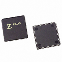
Z16C3516VSG Zilog, Z16C3516VSG Datasheet - Page 83

Z16C3516VSG
Manufacturer Part Number
Z16C3516VSG
Description
IC 16MHZ Z8500 CMOS ISCC 68-PLCC
Manufacturer
Zilog
Series
IUSC™r
Specifications of Z16C3516VSG
Controller Type
Serial Communications Controller (SCC)
Interface
USB
Voltage - Supply
4.75 V ~ 5.25 V
Current - Supply
50mA
Operating Temperature
0°C ~ 70°C
Mounting Type
Surface Mount
Package / Case
68-LCC (J-Lead)
Lead Free Status / RoHS Status
Lead free / RoHS Compliant
Other names
269-4690-5
Z16C3516VSG
Z16C3516VSG
Available stocks
Company
Part Number
Manufacturer
Quantity
Price
Company:
Part Number:
Z16C3516VSG
Manufacturer:
INTEL
Quantity:
6 219
- Current page: 83 of 268
- Download datasheet (3Mb)
UM011001-0601
Bit 5 is the Receiver Overrun Error status
This bit indicates that the receive FIFO has overflowed.
Only the character that has been written over is flagged
with this error, and when the character is read, the Error
condition is latched until reset by the Error Reset com-
mand. The overrun character and all subsequent charac-
ters received until the Error Reset command is issued
causes a Special Receive Condition vector to be returned.
Bit 4 is the Parity Error status
When parity is enabled, this bit is set for the characters
whose parity does not match the programmed sense
(even/odd). This bit is latched so that once an error occurs,
it remains set until the Error Reset command is issued. If
the parity in Special Condition bit is set, a parity error caus-
es a Special Receive Condition vector to be returned on
the character containing the error and on all subsequent
characters until the Error Reset command is issued.
Bits 3, 2, and 1 are the Residue Codes, bits 2, 1, and 0
In those cases in SDLC mode where the received I-Field
is not an integral multiple of the character length, these
three bits indicate the length of the I-Field and are mean-
ingful only for the transfer in which the end of frame bit is
set. This field is set to “011” by a channel or hardware reset
and is forced to this state in Asynchronous mode. These
three bits can leave this state only if SDLC is selected and
a character is received. The codes signify the following
(Reference Table 5-12) when a receive character length is
eight bits per character.
I-Field bits are right-justified in all cases. If a receive char-
acter length other than eight bits is used for the I-Field, a
table similar to Table 5-12 can be constructed for each dif-
ferent character length. Table 5-13 shows the residue
codes for no residue (The I-Field boundary lies on a char-
acter boundary).
Bit 3
1
0
1
0
1
0
1
0
Table 5-12. I-Field Bit Selection (8 Bits Only)
Bit 2
0
1
1
0
0
1
1
0
Bit 1
0
0
0
1
1
1
1
0
in Last Byte
I-Field Bits
0
0
0
0
0
0
1
2
in Previous
I-Field Bits
Byte
P R E L I M I N A R Y
3
4
5
6
7
8
8
8
Bit 0 is the All Sent status
In Asynchronous mode, this bit is set when all characters
have completely cleared the transmitter pins. Most mo-
dems contain additional delays in the data path, which re-
quires the modem control signals to remain active until af-
ter the data has cleared both the transmitter and the
modem. This bit is always set in synchronous and SDLC
modes.
5.5.3 Read Register 2
RR2 contains the interrupt vector written into WR2. When
the register is accessed in Channel A, the vector returned
is the vector actually stored in WR2. When this register is
accessed in Channel B, the vector returned includes sta-
tus information in bits 1, 2 and 3 or in bits 6, 5 and 4, de-
pending on the state of the Status High/Status Low bit in
WR9 and independent of the state of the VIS bit in WR9.
The vector is modified according to Table 5-7 shown in the
explanation of the VIS bit in WR9. If no interrupts are pend-
ing the status is V3,V2,V1 -011, or V6,V5,V4-110. Figure
5-20 shows the bit positions for RR2.
Bits per Character
Table 5-13. Bits per Character Residue Decoding
Read Register 2
D7
* Modified in B Channel
D6
8
7
6
5
D5 D4 D3 D2 D1 D0
Figure 5-20. Read Register 2
Z16C35ISCC™ User’s Manual
Bit 3
0
0
0
0
Register Descriptions
V0
V1
V2
V3
V4
V5
V6
V7
Bit 2
1
0
1
0
Interrupt
Vector *
Bit 1
1
0
0
1
5-23
5
Related parts for Z16C3516VSG
Image
Part Number
Description
Manufacturer
Datasheet
Request
R

Part Number:
Description:
CMOS ISCC INTEGRATED SERIAL COMMUNICATIONS CONTROLLER
Manufacturer:
ZILOG [Zilog, Inc.]
Datasheet:

Part Number:
Description:
Communication Controllers, ZILOG INTELLIGENT PERIPHERAL CONTROLLER (ZIP)
Manufacturer:
Zilog, Inc.
Datasheet:

Part Number:
Description:
KIT DEV FOR Z8 ENCORE 16K TO 64K
Manufacturer:
Zilog
Datasheet:

Part Number:
Description:
KIT DEV Z8 ENCORE XP 28-PIN
Manufacturer:
Zilog
Datasheet:

Part Number:
Description:
DEV KIT FOR Z8 ENCORE 8K/4K
Manufacturer:
Zilog
Datasheet:

Part Number:
Description:
KIT DEV Z8 ENCORE XP 28-PIN
Manufacturer:
Zilog
Datasheet:

Part Number:
Description:
DEV KIT FOR Z8 ENCORE 4K TO 8K
Manufacturer:
Zilog
Datasheet:

Part Number:
Description:
CMOS Z8 microcontroller. ROM 16 Kbytes, RAM 256 bytes, speed 16 MHz, 32 lines I/O, 3.0V to 5.5V
Manufacturer:
Zilog, Inc.
Datasheet:

Part Number:
Description:
Low-cost microcontroller. 512 bytes ROM, 61 bytes RAM, 8 MHz
Manufacturer:
Zilog, Inc.
Datasheet:

Part Number:
Description:
Z8 4K OTP Microcontroller
Manufacturer:
Zilog, Inc.
Datasheet:

Part Number:
Description:
CMOS SUPER8 ROMLESS MCU
Manufacturer:
Zilog, Inc.
Datasheet:

Part Number:
Description:
SL1866 CMOSZ8 OTP Microcontroller
Manufacturer:
Zilog, Inc.
Datasheet:

Part Number:
Description:
SL1866 CMOSZ8 OTP Microcontroller
Manufacturer:
Zilog, Inc.
Datasheet:

Part Number:
Description:
OTP (KB) = 1, RAM = 125, Speed = 12, I/O = 14, 8-bit Timers = 2, Comm Interfaces Other Features = Por, LV Protect, Voltage = 4.5-5.5V
Manufacturer:
Zilog, Inc.
Datasheet:


