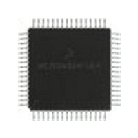
MC68HC705X32CFU Freescale Semiconductor, MC68HC705X32CFU Datasheet - Page 107

MC68HC705X32CFU
Manufacturer Part Number
MC68HC705X32CFU
Description
Manufacturer
Freescale Semiconductor
Datasheet
1.MC68HC705X32CFU.pdf
(232 pages)
Specifications of MC68HC705X32CFU
Cpu Family
HC05
Device Core Size
8b
Frequency (max)
4MHz
Interface Type
SCI
Program Memory Type
EPROM
Program Memory Size
32KB
Total Internal Ram Size
528Byte
# I/os (max)
32
Number Of Timers - General Purpose
1
Operating Supply Voltage (typ)
5V
Operating Supply Voltage (max)
5.5V
Operating Supply Voltage (min)
4.5V
On-chip Adc
8-chx8-bit
Instruction Set Architecture
CISC
Operating Temp Range
-40C to 85C
Operating Temperature Classification
Industrial
Mounting
Surface Mount
Pin Count
64
Package Type
PQFP
Lead Free Status / Rohs Status
Supplier Unconfirmed
Available stocks
Company
Part Number
Manufacturer
Quantity
Price
Part Number:
MC68HC705X32CFU4
Manufacturer:
FREESCALE
Quantity:
20 000
- Current page: 107 of 232
- Download datasheet (6Mb)
7.5
Receive data or transmit data is the serial data that is transferred to the internal data bus from the
receive data input pin (RDI) or from the internal bus to the transmit data output pin (TDO). The
non-return-to-zero (NRZ) data format shown in
criteria:
7.6
The receiver logic hardware also supports a receiver wake-up function which is intended for
systems having more than one receiver. With this function a transmitting device directs messages
to an individual receiver or group of receivers by passing addressing information as the initial
byte(s) of each message. The wake-up function allows receivers not addressed to remain in a
dormant state for the remainder of the unwanted message. This eliminates any further software
overhead to service the remaining characters of the unwanted message and thus improves system
performance.
The receiver is placed in wake-up mode by setting the receiver wake-up bit (RWU) in the SCCR2
register. While RWU is set, all of the receiver related status flags (RDRF, IDLE, OR, NF, and FE)
are inhibited (cannot become set). Note that the idle line detect function is inhibited while the RWU
bit is set. Although RWU may be cleared by a software write to SCCR2, it would be unusual to do
so. Normally RWU is set by software and is cleared automatically in hardware by one of the two
methods described below.
MC68HC05X16
– The idle line is brought to a logic one state prior to transmission/reception of
– A start bit (logic zero) is used to indicate the start of a frame.
– The data is transmitted and received least significant bit first.
– A stop bit (logic one) is used to indicate the end of a frame. A frame consists
– A break is defined as the transmission or reception of a low (logic zero) for at
a character.
of a start bit, a character of eight or nine data bits, and a stop bit.
least one complete frame time (10 zeros for 8-bit format, 11 zeros for 9-bit).
Data format
Receiver wake-up operation
Freescale Semiconductor, Inc.
Idle line
For More Information On This Product,
SERIAL COMMUNICATIONS INTERFACE
Go to: www.freescale.com
Start
Figure 7-3 Data format
0
1
2
Figure 7-3
3
4
5
Control bit M selects
is used and must meet the following
8 or 9 bit data
6
7
8
Stop
Start
0
7-5
7
Related parts for MC68HC705X32CFU
Image
Part Number
Description
Manufacturer
Datasheet
Request
R
Part Number:
Description:
Manufacturer:
Freescale Semiconductor, Inc
Datasheet:
Part Number:
Description:
Manufacturer:
Freescale Semiconductor, Inc
Datasheet:
Part Number:
Description:
Manufacturer:
Freescale Semiconductor, Inc
Datasheet:
Part Number:
Description:
Manufacturer:
Freescale Semiconductor, Inc
Datasheet:
Part Number:
Description:
Manufacturer:
Freescale Semiconductor, Inc
Datasheet:
Part Number:
Description:
Manufacturer:
Freescale Semiconductor, Inc
Datasheet:
Part Number:
Description:
Manufacturer:
Freescale Semiconductor, Inc
Datasheet:
Part Number:
Description:
Manufacturer:
Freescale Semiconductor, Inc
Datasheet:
Part Number:
Description:
Manufacturer:
Freescale Semiconductor, Inc
Datasheet:
Part Number:
Description:
Manufacturer:
Freescale Semiconductor, Inc
Datasheet:
Part Number:
Description:
Manufacturer:
Freescale Semiconductor, Inc
Datasheet:
Part Number:
Description:
Manufacturer:
Freescale Semiconductor, Inc
Datasheet:
Part Number:
Description:
Manufacturer:
Freescale Semiconductor, Inc
Datasheet:
Part Number:
Description:
Manufacturer:
Freescale Semiconductor, Inc
Datasheet:
Part Number:
Description:
Manufacturer:
Freescale Semiconductor, Inc
Datasheet:


