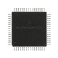
MC68HC705X32CFU Freescale Semiconductor, MC68HC705X32CFU Datasheet - Page 201

MC68HC705X32CFU
Manufacturer Part Number
MC68HC705X32CFU
Description
Manufacturer
Freescale Semiconductor
Datasheet
1.MC68HC705X32CFU.pdf
(232 pages)
Specifications of MC68HC705X32CFU
Cpu Family
HC05
Device Core Size
8b
Frequency (max)
4MHz
Interface Type
SCI
Program Memory Type
EPROM
Program Memory Size
32KB
Total Internal Ram Size
528Byte
# I/os (max)
32
Number Of Timers - General Purpose
1
Operating Supply Voltage (typ)
5V
Operating Supply Voltage (max)
5.5V
Operating Supply Voltage (min)
4.5V
On-chip Adc
8-chx8-bit
Instruction Set Architecture
CISC
Operating Temp Range
-40C to 85C
Operating Temperature Classification
Industrial
Mounting
Surface Mount
Pin Count
64
Package Type
PQFP
Lead Free Status / Rohs Status
Supplier Unconfirmed
Available stocks
Company
Part Number
Manufacturer
Quantity
Price
Part Number:
MC68HC705X32CFU4
Manufacturer:
FREESCALE
Quantity:
20 000
- Current page: 201 of 232
- Download datasheet (6Mb)
B.8.1
If a non $00 byte is detected, the red LED will be turned on and the routine will stop (see
Figure
on. PD1 is then checked. If PD1=0, the bootstrap program stops here and no programming occurs
until a high level is sensed on PD1.
If PD1 = 1, the bootstrap program proceeds to erase the EEPROM1 for a nominal 2.5 seconds (4.0
MHz crystal). It is then checked for complete erasure; if any EEPROM byte is not erased, the
program will stop before erasing the SEC byte. When both EPROM and EEPROM1 are completely
erased and the security bit is cleared the programming operation can be performed. A schematic
diagram of the circuit required for erased EPROM verification is shown in
B.8.2
Within this mode there are various subsections which can be utilised by correctly configuring the
port pins shown in
The erased EPROM verification program will be executed first as described in
PD2=0, the programming time is set to 5 milliseconds with the bootstrap program and verify for the
EPROM taking approximately 15 seconds. The EPROM will be loaded in increasing address order
with non EPROM segments being skipped by the loader. Simultaneous programming is performed
by reading sixteen bytes of data before actual programming is performed, thus dividing the loading
time of the internal EPROM by 16. If any block of 16 EPROM bytes or 1 EEPROM byte of data is
in the erased state, no programming takes place, thus speeding up the execution time.
Parallel data is entered through Port A, while the 15-bit address is output on port B, PC0 to PC4
and TCMP1 and TCMP2. If the data comes from an external EPROM, the handshake can be
disabled by connecting together PC5 and PC6. If the data is supplied by a parallel interface,
handshake will be provided by PC5 and PC6 according to the timing diagram of
also
During programming, the green LED will flash at about 3 Hz.
Upon completion of the programming operation, the EPROM and EEPROM1 content will be
checked against the external data source. If programming is verified the green LED will stay on,
while an error will cause the red LED to be turned on.
which can be used to program the EPROM or to load and execute data in the RAM.
Note:
MC68HC05X16
Figure
B-3). Only when the whole EPROM array is verified as erased will the green LED be turned
The entire EPROM and EEPROM1 can be loaded from the external source; if it is
desired to leave a segment undisturbed, the data for this segment should be all $00s
for EPROM data and all $FFs for EEPROM1 data.
B-5).
Erased EPROM verification and EEPROM erasure
EPROM/EEPROM parallel bootstrap
Freescale Semiconductor, Inc.
Table
For More Information On This Product,
B-5.
Go to: www.freescale.com
MC68HC705X32
Figure B-6
is a schematic diagram of a circuit
Figure
Section
B-6.
Figure B-4
B.8.1. When
B-17
(see
15
Related parts for MC68HC705X32CFU
Image
Part Number
Description
Manufacturer
Datasheet
Request
R
Part Number:
Description:
Manufacturer:
Freescale Semiconductor, Inc
Datasheet:
Part Number:
Description:
Manufacturer:
Freescale Semiconductor, Inc
Datasheet:
Part Number:
Description:
Manufacturer:
Freescale Semiconductor, Inc
Datasheet:
Part Number:
Description:
Manufacturer:
Freescale Semiconductor, Inc
Datasheet:
Part Number:
Description:
Manufacturer:
Freescale Semiconductor, Inc
Datasheet:
Part Number:
Description:
Manufacturer:
Freescale Semiconductor, Inc
Datasheet:
Part Number:
Description:
Manufacturer:
Freescale Semiconductor, Inc
Datasheet:
Part Number:
Description:
Manufacturer:
Freescale Semiconductor, Inc
Datasheet:
Part Number:
Description:
Manufacturer:
Freescale Semiconductor, Inc
Datasheet:
Part Number:
Description:
Manufacturer:
Freescale Semiconductor, Inc
Datasheet:
Part Number:
Description:
Manufacturer:
Freescale Semiconductor, Inc
Datasheet:
Part Number:
Description:
Manufacturer:
Freescale Semiconductor, Inc
Datasheet:
Part Number:
Description:
Manufacturer:
Freescale Semiconductor, Inc
Datasheet:
Part Number:
Description:
Manufacturer:
Freescale Semiconductor, Inc
Datasheet:
Part Number:
Description:
Manufacturer:
Freescale Semiconductor, Inc
Datasheet:


