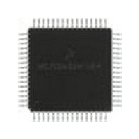
MC68HC705X32CFU Freescale Semiconductor, MC68HC705X32CFU Datasheet - Page 108

MC68HC705X32CFU
Manufacturer Part Number
MC68HC705X32CFU
Description
Manufacturer
Freescale Semiconductor
Datasheet
1.MC68HC705X32CFU.pdf
(232 pages)
Specifications of MC68HC705X32CFU
Cpu Family
HC05
Device Core Size
8b
Frequency (max)
4MHz
Interface Type
SCI
Program Memory Type
EPROM
Program Memory Size
32KB
Total Internal Ram Size
528Byte
# I/os (max)
32
Number Of Timers - General Purpose
1
Operating Supply Voltage (typ)
5V
Operating Supply Voltage (max)
5.5V
Operating Supply Voltage (min)
4.5V
On-chip Adc
8-chx8-bit
Instruction Set Architecture
CISC
Operating Temp Range
-40C to 85C
Operating Temperature Classification
Industrial
Mounting
Surface Mount
Pin Count
64
Package Type
PQFP
Lead Free Status / Rohs Status
Supplier Unconfirmed
Available stocks
Company
Part Number
Manufacturer
Quantity
Price
Part Number:
MC68HC705X32CFU4
Manufacturer:
FREESCALE
Quantity:
20 000
- Current page: 108 of 232
- Download datasheet (6Mb)
7
7.6.1
In idle line wake-up mode, a dormant receiver wakes up as soon as the RDI line becomes idle. Idle
is defined as a continuous logic high level on the RDI line for ten (or eleven) full bit times. Systems
using this type of wake-up must provide at least one character time of idle between messages to
wake up sleeping receivers, but must not allow any idle time between characters within a message.
7.6.2
In address mark wake-up, the most significant bit (MSB) in a character is used to indicate whether
it is an address (1) or data (0) character. Sleeping receivers will wake up whenever an address
character is received. Systems using this method for wake-up would set the MSB of the first
character of each message and leave it clear for all other characters in the message. Idle periods
may be present within messages and no idle time is required between messages for this wake-up
method.
7.7
Receive data is the serial data that is applied through the input line and the SCI to the internal bus.
The receiver circuitry clocks the input at a rate equal to 16 times the baud rate. This time is referred
to as the RT rate in
The receiver clock generator is controlled by the baud rate register, as shown in
Figure
Once a valid start bit is detected, the start bit, each data bit and the stop bit are sampled three
times at RT intervals 8 RT, 9 RT and 10 RT (1 RT is the position where the bit is expected to start),
as shown in
the majority of the samples. A noise flag is set when all three samples on a valid start bit or data
bit or the stop bit do not agree.
7.8
When the input (idle) line is detected low, it is tested for three more sample times (referred to as
the start edge verification samples in
detect a logic zero, a valid start bit has been detected, otherwise the line is assumed to be idle. A
noise flag is set if one of the three verification samples detect a logic one, thus a valid start bit could
be assumed with a set noise flag present.
If there has been a framing error without detection of a break (10 zeros for 8 bit format or 11 zeros
for 9 bit format), the circuit continues to operate as if there actually was a stop bit, and the start
7-2; however, the SCI is synchronized by the start bit, independent of the transmitter.
Figure
Idle line wake-up
Address mark wake-up
Receive data in (RDI)
Start bit detection
Freescale Semiconductor, Inc.
7-5. The value of the bit is determined by voting logic which takes the value of
Figure 7-4
For More Information On This Product,
SERIAL COMMUNICATIONS INTERFACE
and as the receiver clock in
Go to: www.freescale.com
Figure
7-4). If at least two of these three verification samples
Figure
7-2.
MC68HC05X16
Figure 7-1
Rev. 1
and
Related parts for MC68HC705X32CFU
Image
Part Number
Description
Manufacturer
Datasheet
Request
R
Part Number:
Description:
Manufacturer:
Freescale Semiconductor, Inc
Datasheet:
Part Number:
Description:
Manufacturer:
Freescale Semiconductor, Inc
Datasheet:
Part Number:
Description:
Manufacturer:
Freescale Semiconductor, Inc
Datasheet:
Part Number:
Description:
Manufacturer:
Freescale Semiconductor, Inc
Datasheet:
Part Number:
Description:
Manufacturer:
Freescale Semiconductor, Inc
Datasheet:
Part Number:
Description:
Manufacturer:
Freescale Semiconductor, Inc
Datasheet:
Part Number:
Description:
Manufacturer:
Freescale Semiconductor, Inc
Datasheet:
Part Number:
Description:
Manufacturer:
Freescale Semiconductor, Inc
Datasheet:
Part Number:
Description:
Manufacturer:
Freescale Semiconductor, Inc
Datasheet:
Part Number:
Description:
Manufacturer:
Freescale Semiconductor, Inc
Datasheet:
Part Number:
Description:
Manufacturer:
Freescale Semiconductor, Inc
Datasheet:
Part Number:
Description:
Manufacturer:
Freescale Semiconductor, Inc
Datasheet:
Part Number:
Description:
Manufacturer:
Freescale Semiconductor, Inc
Datasheet:
Part Number:
Description:
Manufacturer:
Freescale Semiconductor, Inc
Datasheet:
Part Number:
Description:
Manufacturer:
Freescale Semiconductor, Inc
Datasheet:


