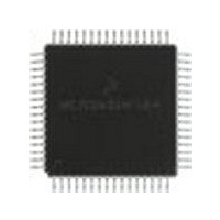
MC68HC705X32CFU Freescale Semiconductor, MC68HC705X32CFU Datasheet - Page 56

MC68HC705X32CFU
Manufacturer Part Number
MC68HC705X32CFU
Description
Manufacturer
Freescale Semiconductor
Datasheet
1.MC68HC705X32CFU.pdf
(232 pages)
Specifications of MC68HC705X32CFU
Cpu Family
HC05
Device Core Size
8b
Frequency (max)
4MHz
Interface Type
SCI
Program Memory Type
EPROM
Program Memory Size
32KB
Total Internal Ram Size
528Byte
# I/os (max)
32
Number Of Timers - General Purpose
1
Operating Supply Voltage (typ)
5V
Operating Supply Voltage (max)
5.5V
Operating Supply Voltage (min)
4.5V
On-chip Adc
8-chx8-bit
Instruction Set Architecture
CISC
Operating Temp Range
-40C to 85C
Operating Temperature Classification
Industrial
Mounting
Surface Mount
Pin Count
64
Package Type
PQFP
Lead Free Status / Rohs Status
Supplier Unconfirmed
Available stocks
Company
Part Number
Manufacturer
Quantity
Price
Part Number:
MC68HC705X32CFU4
Manufacturer:
FREESCALE
Quantity:
20 000
- Current page: 56 of 232
- Download datasheet (6Mb)
4
Table 4-1
that the read/write signal shown is internal and not available to the user.
4.2
These ports are standard M68HC05 bidirectional I/O ports, each comprising a data register and a
data direction register.
Reset does not affect the state of the data register, but clears the data direction register, thereby
returning all port pins to input mode. Writing a ‘1’ to any DDR bit sets the corresponding port pin
to output mode.
Wired-OR interrupts are provided on all pins of port B. If WOIE is enabled, any combination of high
logic levels on port B pins which are programmed as inputs will trigger an external interrupt. See
Section
10.2.3.2.
shows the effect of reading from or writing to an I/O pin in various circumstances. Note
R/W
0
0
1
1
Data direction
Latched data
Ports A and B
register bit
register bit
DDRn
Freescale Semiconductor, Inc.
0
1
0
1
The I/O pin is in input mode. Data is written into the output data latch.
Data is written into the output data latch, and output to the I/O pin.
The state of the I/O pin is read.
The I/O pin is in output mode. The output data latch is read.
For More Information On This Product,
buffer
Figure 4-1 Standard I/O port structure
data
O/P
DDRn
DATA
Go to: www.freescale.com
INPUT/OUTPUT PORTS
Table 4-1 I/O pin states
Action of MCU write to/read of data bit
buffer
Input
Output
buffer
Pin
I/O
Output
Input
DDRn
1
1
0
0
MC68HC05X16
DATA
0
1
0
1
I/O Pin
tristate
tristate
0
1
Rev. 1
Related parts for MC68HC705X32CFU
Image
Part Number
Description
Manufacturer
Datasheet
Request
R
Part Number:
Description:
Manufacturer:
Freescale Semiconductor, Inc
Datasheet:
Part Number:
Description:
Manufacturer:
Freescale Semiconductor, Inc
Datasheet:
Part Number:
Description:
Manufacturer:
Freescale Semiconductor, Inc
Datasheet:
Part Number:
Description:
Manufacturer:
Freescale Semiconductor, Inc
Datasheet:
Part Number:
Description:
Manufacturer:
Freescale Semiconductor, Inc
Datasheet:
Part Number:
Description:
Manufacturer:
Freescale Semiconductor, Inc
Datasheet:
Part Number:
Description:
Manufacturer:
Freescale Semiconductor, Inc
Datasheet:
Part Number:
Description:
Manufacturer:
Freescale Semiconductor, Inc
Datasheet:
Part Number:
Description:
Manufacturer:
Freescale Semiconductor, Inc
Datasheet:
Part Number:
Description:
Manufacturer:
Freescale Semiconductor, Inc
Datasheet:
Part Number:
Description:
Manufacturer:
Freescale Semiconductor, Inc
Datasheet:
Part Number:
Description:
Manufacturer:
Freescale Semiconductor, Inc
Datasheet:
Part Number:
Description:
Manufacturer:
Freescale Semiconductor, Inc
Datasheet:
Part Number:
Description:
Manufacturer:
Freescale Semiconductor, Inc
Datasheet:
Part Number:
Description:
Manufacturer:
Freescale Semiconductor, Inc
Datasheet:


