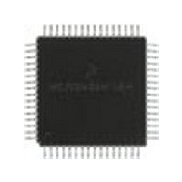
MC68HC705X32CFU Freescale Semiconductor, MC68HC705X32CFU Datasheet - Page 96

MC68HC705X32CFU
Manufacturer Part Number
MC68HC705X32CFU
Description
Manufacturer
Freescale Semiconductor
Datasheet
1.MC68HC705X32CFU.pdf
(232 pages)
Specifications of MC68HC705X32CFU
Cpu Family
HC05
Device Core Size
8b
Frequency (max)
4MHz
Interface Type
SCI
Program Memory Type
EPROM
Program Memory Size
32KB
Total Internal Ram Size
528Byte
# I/os (max)
32
Number Of Timers - General Purpose
1
Operating Supply Voltage (typ)
5V
Operating Supply Voltage (max)
5.5V
Operating Supply Voltage (min)
4.5V
On-chip Adc
8-chx8-bit
Instruction Set Architecture
CISC
Operating Temp Range
-40C to 85C
Operating Temperature Classification
Industrial
Mounting
Surface Mount
Pin Count
64
Package Type
PQFP
Lead Free Status / Rohs Status
Supplier Unconfirmed
Available stocks
Company
Part Number
Manufacturer
Quantity
Price
Part Number:
MC68HC705X32CFU4
Manufacturer:
FREESCALE
Quantity:
20 000
- Current page: 96 of 232
- Download datasheet (6Mb)
6
The result obtained from an input capture will be one greater than the value of the free-running
counter on the rising edge of the internal bus clock preceding the external transition. This delay is
required for internal synchronization. Resolution is one count of the free-running counter, which is
four internal bus clock cycles. The free-running counter contents are transferred to the input
capture register 1 on each valid signal transition whether the input capture 1 flag (ICF1) is set or
clear. The input capture register 1 always contains the free-running counter value that corresponds
to the most recent input capture 1. After a read of the input capture 1 register MSB ($14), the
counter transfer is inhibited until the LSB ($15) is also read. This characteristic causes the time
used in the input capture software routine and its interaction with the main program to determine
the minimum pulse period. A read of the input capture 1 register LSB ($15) does not inhibit the
free-running counter transfer since the two actions occur on opposite edges of the internal bus
clock.
Reset does not affect the contents of the input capture 1 register, except when exiting STOP mode
(see
6.3.2
The two 8-bit registers that make up the 16-bit input capture register 2 are read-only, and are used
to latch the value of the free-running counter after the input capture edge detector circuit 2 senses
a negative transition at pin TCAP2. When an input capture 2 occurs, the corresponding flag ICF2
in TSR is set. An interrupt can also accompany an input capture 2 provided the ICIE bit in TCR is
set.The 8 most significant bits are stored in the input capture 2 high register at $1C, the 8 least
significant bits in the input capture 2 low register at $1D.
The result obtained from an input capture will be one greater than the value of the free-running
counter on the rising edge of the internal bus clock preceding the external transition. This delay is
required for internal synchronization. Resolution is one count of the free-running counter, which is
four internal bus clock cycles. The free-running counter contents are transferred to the input
capture register 2 on each negative signal transition whether the input capture 2 flag (IC2F) is set
or clear. The input capture register 2 always contains the free-running counter value that
corresponds to the most recent input capture 2. After a read of the input capture register 2 MSB
($1C), the counter transfer is inhibited until the LSB ($1D) is also read. This characteristic causes
the time used in the input capture software routine and its interaction with the main program to
determine the minimum pulse period. A read of the input capture register 2 LSB ($1C) does not
inhibit the free-running counter transfer since the two actions occur on opposite edges of the
internal bus clock.
Reset does not affect the contents of the input capture 2 register, except when exiting STOP mode
(see
Section
Section
Input capture high 2
Input capture low 2
6.6).
6.6).
Input capture register 2 (ICR2)
Freescale Semiconductor, Inc.
For More Information On This Product,
Address
$001C
$001D
Go to: www.freescale.com
PROGRAMMABLE TIMER
bit 7
bit 6
bit 5
bit 4
bit 3
bit 2
bit 1
MC68HC05X16
bit 0
Undefined
Undefined
on reset
State
Rev. 1
Related parts for MC68HC705X32CFU
Image
Part Number
Description
Manufacturer
Datasheet
Request
R
Part Number:
Description:
Manufacturer:
Freescale Semiconductor, Inc
Datasheet:
Part Number:
Description:
Manufacturer:
Freescale Semiconductor, Inc
Datasheet:
Part Number:
Description:
Manufacturer:
Freescale Semiconductor, Inc
Datasheet:
Part Number:
Description:
Manufacturer:
Freescale Semiconductor, Inc
Datasheet:
Part Number:
Description:
Manufacturer:
Freescale Semiconductor, Inc
Datasheet:
Part Number:
Description:
Manufacturer:
Freescale Semiconductor, Inc
Datasheet:
Part Number:
Description:
Manufacturer:
Freescale Semiconductor, Inc
Datasheet:
Part Number:
Description:
Manufacturer:
Freescale Semiconductor, Inc
Datasheet:
Part Number:
Description:
Manufacturer:
Freescale Semiconductor, Inc
Datasheet:
Part Number:
Description:
Manufacturer:
Freescale Semiconductor, Inc
Datasheet:
Part Number:
Description:
Manufacturer:
Freescale Semiconductor, Inc
Datasheet:
Part Number:
Description:
Manufacturer:
Freescale Semiconductor, Inc
Datasheet:
Part Number:
Description:
Manufacturer:
Freescale Semiconductor, Inc
Datasheet:
Part Number:
Description:
Manufacturer:
Freescale Semiconductor, Inc
Datasheet:
Part Number:
Description:
Manufacturer:
Freescale Semiconductor, Inc
Datasheet:


