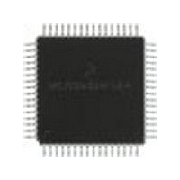
MC68HC705X32CFU Freescale Semiconductor, MC68HC705X32CFU Datasheet - Page 112

MC68HC705X32CFU
Manufacturer Part Number
MC68HC705X32CFU
Description
Manufacturer
Freescale Semiconductor
Datasheet
1.MC68HC705X32CFU.pdf
(232 pages)
Specifications of MC68HC705X32CFU
Cpu Family
HC05
Device Core Size
8b
Frequency (max)
4MHz
Interface Type
SCI
Program Memory Type
EPROM
Program Memory Size
32KB
Total Internal Ram Size
528Byte
# I/os (max)
32
Number Of Timers - General Purpose
1
Operating Supply Voltage (typ)
5V
Operating Supply Voltage (max)
5.5V
Operating Supply Voltage (min)
4.5V
On-chip Adc
8-chx8-bit
Instruction Set Architecture
CISC
Operating Temp Range
-40C to 85C
Operating Temperature Classification
Industrial
Mounting
Surface Mount
Pin Count
64
Package Type
PQFP
Lead Free Status / Rohs Status
Supplier Unconfirmed
Available stocks
Company
Part Number
Manufacturer
Quantity
Price
Part Number:
MC68HC705X32CFU4
Manufacturer:
FREESCALE
Quantity:
20 000
- Current page: 112 of 232
- Download datasheet (6Mb)
7
7.11
The SCI system is configured and controlled by five registers: SCDR, SCCR1, SCCR2, SCSR,
and BAUD.
7.11.1
The SCDR is controlled by the internal R/W signal and performs two functions in the SCI. It acts
as the receive data register (RDR) when it is read and as the transmit data register (TDR) when it
is written.
provides the interface from the receive shift register to the internal data bus and the TDR provides
the parallel interface from the internal data bus to the transmit shift register.
The receive data register is a read-only register containing the last byte of data received from the
shift register for the internal data bus. The RDR full bit (RDRF) in the serial communications status
register is set to indicate that a byte has been transferred from the input serial shift register to the
SCDR. The transfer is synchronized with the receiver bit rate clock (from the receiver control) as
shown in
The transmit data register (TDR) is a write-only register containing the next byte of data to be
applied to the transmit shift register from the internal data bus. As long as the transmitter is
enabled, data stored in the SCDR is transferred to the transmit shift register (after the current byte
in the shift register has been transmitted).
The transfer is synchronized with the transmitter bit rate clock (from the transmitter control) as
shown in
7.11.2
The SCI control register 1 (SCCR1) contains control bits related to the nine data bit character
format, the receiver wake-up feature and the options to output the transmitter clocks for
synchronous transmissions.
SCI control 1 (SCCR1)
SCI data (SCDR)
Figure
Figure
Figure 7-1
SCI registers
Serial communications data register (SCDR)
Serial communications control register 1 (SCCR1)
7-1. All data is received with the least significant bit first.
7-1. All data is received with the least significant bit first.
Freescale Semiconductor, Inc.
shows this register as two separate registers, RDR and TDR. The RDR
For More Information On This Product,
SERIAL COMMUNICATIONS INTERFACE
Address
Address
$000E
$0011
Go to: www.freescale.com
bit 7
bit 7
R8
bit 6
bit 6
T8
bit 5
bit 5
bit 4
bit 4
M
WAKE CPOL CPHA LBCL Undefined
bit 3
bit 3
bit 2
bit 2
bit 1
bit 1
MC68HC05X16
bit 0
bit 0
0000 0000
on reset
on reset
State
State
Rev. 1
Related parts for MC68HC705X32CFU
Image
Part Number
Description
Manufacturer
Datasheet
Request
R
Part Number:
Description:
Manufacturer:
Freescale Semiconductor, Inc
Datasheet:
Part Number:
Description:
Manufacturer:
Freescale Semiconductor, Inc
Datasheet:
Part Number:
Description:
Manufacturer:
Freescale Semiconductor, Inc
Datasheet:
Part Number:
Description:
Manufacturer:
Freescale Semiconductor, Inc
Datasheet:
Part Number:
Description:
Manufacturer:
Freescale Semiconductor, Inc
Datasheet:
Part Number:
Description:
Manufacturer:
Freescale Semiconductor, Inc
Datasheet:
Part Number:
Description:
Manufacturer:
Freescale Semiconductor, Inc
Datasheet:
Part Number:
Description:
Manufacturer:
Freescale Semiconductor, Inc
Datasheet:
Part Number:
Description:
Manufacturer:
Freescale Semiconductor, Inc
Datasheet:
Part Number:
Description:
Manufacturer:
Freescale Semiconductor, Inc
Datasheet:
Part Number:
Description:
Manufacturer:
Freescale Semiconductor, Inc
Datasheet:
Part Number:
Description:
Manufacturer:
Freescale Semiconductor, Inc
Datasheet:
Part Number:
Description:
Manufacturer:
Freescale Semiconductor, Inc
Datasheet:
Part Number:
Description:
Manufacturer:
Freescale Semiconductor, Inc
Datasheet:
Part Number:
Description:
Manufacturer:
Freescale Semiconductor, Inc
Datasheet:


