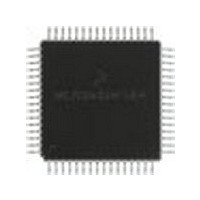
MC68HC705X32CFU Freescale Semiconductor, MC68HC705X32CFU Datasheet - Page 99

MC68HC705X32CFU
Manufacturer Part Number
MC68HC705X32CFU
Description
Manufacturer
Freescale Semiconductor
Datasheet
1.MC68HC705X32CFU.pdf
(232 pages)
Specifications of MC68HC705X32CFU
Cpu Family
HC05
Device Core Size
8b
Frequency (max)
4MHz
Interface Type
SCI
Program Memory Type
EPROM
Program Memory Size
32KB
Total Internal Ram Size
528Byte
# I/os (max)
32
Number Of Timers - General Purpose
1
Operating Supply Voltage (typ)
5V
Operating Supply Voltage (max)
5.5V
Operating Supply Voltage (min)
4.5V
On-chip Adc
8-chx8-bit
Instruction Set Architecture
CISC
Operating Temp Range
-40C to 85C
Operating Temperature Classification
Industrial
Mounting
Surface Mount
Pin Count
64
Package Type
PQFP
Lead Free Status / Rohs Status
Supplier Unconfirmed
Available stocks
Company
Part Number
Manufacturer
Quantity
Price
Part Number:
MC68HC705X32CFU4
Manufacturer:
FREESCALE
Quantity:
20 000
- Current page: 99 of 232
- Download datasheet (6Mb)
The purpose of this procedure is to prevent the OCF1 bit from being set between the time it is read
and the write to the corresponding output compare register.
All bits of the output compare register are readable and writable and are not altered by the timer
hardware or reset. If the compare function is not needed, the two bytes of the output compare
register can be used as storage locations.
6.4.3
A software force compare is required in many applications. To achieve this, bit 3 (FOLV1 for OCR1)
and bit 4 (FOLV2 for OCR2) in the timer control register are used. These bits always read as ‘zero’,
but a write to ‘one’ causes the respective OLVL1 or OLVL2 values to be copied to the respective
output level (TCMP1 and TCMP2 pins).
Internal logic is arranged such that in a single instruction, one can change OLVL1 and/or OLVL2,
at the same time causing a forced output compare with the new values of OLVL1 and OLVL2. In
conjunction with normal compare, this function allows a wide range of applications including fixed
frequency generation.
Note:
6.5
The programmable timer works in conjunction with the PLM system to execute two 8-bit D/A PLM
conversions, with a choice of two repetition rates (see
6.5.1
MC68HC05X16
Pulse length modulation A (PLMA)
Pulse length modulation B (PLMB)
A software force compare will affect the corresponding output pin TCMP1 and/or
TCMP2, but will not affect the compare flag, thus it will not generate an interrupt.
Software force compare
Pulse length modulation (PLM)
Pulse length modulation registers A and B (PLMA/PLMB)
Freescale Semiconductor, Inc.
For More Information On This Product,
Address
Address
Go to: www.freescale.com
$000A
$000B
PROGRAMMABLE TIMER
bit 7
bit 7
bit 6
bit 6
bit 5
bit 5
Section
bit 4
bit 4
8).
bit 3
bit 3
bit 2
bit 2
bit 1
bit 1
bit 0
bit 0
0000 0000
0000 0000
on reset
on reset
State
State
6-11
6
Related parts for MC68HC705X32CFU
Image
Part Number
Description
Manufacturer
Datasheet
Request
R
Part Number:
Description:
Manufacturer:
Freescale Semiconductor, Inc
Datasheet:
Part Number:
Description:
Manufacturer:
Freescale Semiconductor, Inc
Datasheet:
Part Number:
Description:
Manufacturer:
Freescale Semiconductor, Inc
Datasheet:
Part Number:
Description:
Manufacturer:
Freescale Semiconductor, Inc
Datasheet:
Part Number:
Description:
Manufacturer:
Freescale Semiconductor, Inc
Datasheet:
Part Number:
Description:
Manufacturer:
Freescale Semiconductor, Inc
Datasheet:
Part Number:
Description:
Manufacturer:
Freescale Semiconductor, Inc
Datasheet:
Part Number:
Description:
Manufacturer:
Freescale Semiconductor, Inc
Datasheet:
Part Number:
Description:
Manufacturer:
Freescale Semiconductor, Inc
Datasheet:
Part Number:
Description:
Manufacturer:
Freescale Semiconductor, Inc
Datasheet:
Part Number:
Description:
Manufacturer:
Freescale Semiconductor, Inc
Datasheet:
Part Number:
Description:
Manufacturer:
Freescale Semiconductor, Inc
Datasheet:
Part Number:
Description:
Manufacturer:
Freescale Semiconductor, Inc
Datasheet:
Part Number:
Description:
Manufacturer:
Freescale Semiconductor, Inc
Datasheet:
Part Number:
Description:
Manufacturer:
Freescale Semiconductor, Inc
Datasheet:


