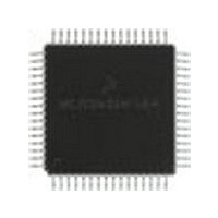
MC68HC705X32CFU Freescale Semiconductor, MC68HC705X32CFU Datasheet - Page 165

MC68HC705X32CFU
Manufacturer Part Number
MC68HC705X32CFU
Description
Manufacturer
Freescale Semiconductor
Datasheet
1.MC68HC705X32CFU.pdf
(232 pages)
Specifications of MC68HC705X32CFU
Cpu Family
HC05
Device Core Size
8b
Frequency (max)
4MHz
Interface Type
SCI
Program Memory Type
EPROM
Program Memory Size
32KB
Total Internal Ram Size
528Byte
# I/os (max)
32
Number Of Timers - General Purpose
1
Operating Supply Voltage (typ)
5V
Operating Supply Voltage (max)
5.5V
Operating Supply Voltage (min)
4.5V
On-chip Adc
8-chx8-bit
Instruction Set Architecture
CISC
Operating Temp Range
-40C to 85C
Operating Temperature Classification
Industrial
Mounting
Surface Mount
Pin Count
64
Package Type
PQFP
Lead Free Status / Rohs Status
Supplier Unconfirmed
Available stocks
Company
Part Number
Manufacturer
Quantity
Price
Part Number:
MC68HC705X32CFU4
Manufacturer:
FREESCALE
Quantity:
20 000
- Current page: 165 of 232
- Download datasheet (6Mb)
MC68HC05X16
(1) All I
(2) Typical values are at mid point of voltage range and at 25 C only.
(3) RUN and WAIT I
(4) f
(5) f
(6) These limits are also applicable under the following conditions:
(7) These limits are also applicable under the following conditions:
(8) These currents are the summation of the MCU current + CAN current (I
(9) Current injection is guaranteed but not tested.
(V
Input current
Input current
Input current
Capacitance
DC injection current
DD
switching currents inherent in CMOS designs (see Section 2).
from rail; no DC loads; maximum load on outputs 50pF (20pF on OSC2).
STOP/WAIT I
OSC1 = V
MCU RUN mode/SLOW mode/CAN active
MCU WAIT mode/SLOW mode/CAN active
MCU WAIT mode/CAN active
MCU WAIT mode/SLOW mode/CAN asleep
Functionality of the MCU is guaranteed during injection of dc current up to the maximum specified level.
The maximum specified current for each port is the sum of the magnitudes of the currents on each side of the
individual port pins.
Some disturbance of the A/D accuracy is possible during an injection event and is dependent on board layout,
power supply decoupling and reference voltage decoupling configurations.
OSC
OSC
IRQ, TCAP1, TCAP2, RDI,
PD0/AN0-PD7/AN7 (channel not selected)
Ports (as input or output), RESET, TDO, SCLK
IRQ, TCAP1, TCAP2, OSC1, RDI
PD0/AN0–PD7/AN7 (A/D off)
PD0/AN0–PD7/AN7 (A/D on)
Port A (PA0–PA7)
Port B (PB0–PB7)
OSC1=V
OSC1=V
= 5.0 Vdc
DD
= 4.4 MHz; f
= 22 MHz; f
measurements taken with suitable decoupling capacitors across the power supply to suppress the transient
Freescale Semiconductor, Inc.
DD
DD
SS
. WAIT I
DD
(OSC2=V
(OSC2=V
10%, V
Characteristic
: all ports configured as inputs; V
DD
(9)
BUS
BUS
For More Information On This Product,
: measured using an external square-wave clock source, refer to
DD
= 2.2 MHz; f
= 2.2 MHz; f
SS
DD
is affected linearly by the OSC2 capacitance.
SS
= 0 Vdc, T
)
)
Table 12-2 DC electrical characteristics
Go to: www.freescale.com
(1)
ELECTRICAL SPECIFICATIONS
CAN
CAN
A
= –40 C to +125 C)
= 11 MHz
= 2.2 MHz
IL
= 0.2 V and V
Symbol
C
|I
|I
C
C
C
I
I
I
OUT
FH
INJ
INJ
FL
IN
IN
IN
IN
|
|
IH
= V
– 10
DD
Min
—
—
—
—
—
—
—
—
DD
– 0.2 V: STOP I
+ I
DD1
)
Typ
—
—
—
—
12
22
—
—
Figure
0.2
(2)
DD
2-6(c); all inputs 0.2 V
measured with
Max
+10
12
10
10
—
—
—
8
1
Unit
mA
mA
pF
pF
pF
pF
A
A
12-3
12
Related parts for MC68HC705X32CFU
Image
Part Number
Description
Manufacturer
Datasheet
Request
R
Part Number:
Description:
Manufacturer:
Freescale Semiconductor, Inc
Datasheet:
Part Number:
Description:
Manufacturer:
Freescale Semiconductor, Inc
Datasheet:
Part Number:
Description:
Manufacturer:
Freescale Semiconductor, Inc
Datasheet:
Part Number:
Description:
Manufacturer:
Freescale Semiconductor, Inc
Datasheet:
Part Number:
Description:
Manufacturer:
Freescale Semiconductor, Inc
Datasheet:
Part Number:
Description:
Manufacturer:
Freescale Semiconductor, Inc
Datasheet:
Part Number:
Description:
Manufacturer:
Freescale Semiconductor, Inc
Datasheet:
Part Number:
Description:
Manufacturer:
Freescale Semiconductor, Inc
Datasheet:
Part Number:
Description:
Manufacturer:
Freescale Semiconductor, Inc
Datasheet:
Part Number:
Description:
Manufacturer:
Freescale Semiconductor, Inc
Datasheet:
Part Number:
Description:
Manufacturer:
Freescale Semiconductor, Inc
Datasheet:
Part Number:
Description:
Manufacturer:
Freescale Semiconductor, Inc
Datasheet:
Part Number:
Description:
Manufacturer:
Freescale Semiconductor, Inc
Datasheet:
Part Number:
Description:
Manufacturer:
Freescale Semiconductor, Inc
Datasheet:
Part Number:
Description:
Manufacturer:
Freescale Semiconductor, Inc
Datasheet:


