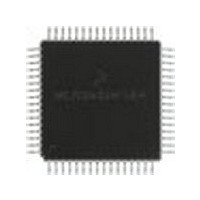
MC68HC705X32CFU Freescale Semiconductor, MC68HC705X32CFU Datasheet - Page 224

MC68HC705X32CFU
Manufacturer Part Number
MC68HC705X32CFU
Description
Manufacturer
Freescale Semiconductor
Datasheet
1.MC68HC705X32CFU.pdf
(232 pages)
Specifications of MC68HC705X32CFU
Cpu Family
HC05
Device Core Size
8b
Frequency (max)
4MHz
Interface Type
SCI
Program Memory Type
EPROM
Program Memory Size
32KB
Total Internal Ram Size
528Byte
# I/os (max)
32
Number Of Timers - General Purpose
1
Operating Supply Voltage (typ)
5V
Operating Supply Voltage (max)
5.5V
Operating Supply Voltage (min)
4.5V
On-chip Adc
8-chx8-bit
Instruction Set Architecture
CISC
Operating Temp Range
-40C to 85C
Operating Temperature Classification
Industrial
Mounting
Surface Mount
Pin Count
64
Package Type
PQFP
Lead Free Status / Rohs Status
Supplier Unconfirmed
Available stocks
Company
Part Number
Manufacturer
Quantity
Price
Part Number:
MC68HC705X32CFU4
Manufacturer:
FREESCALE
Quantity:
20 000
- Current page: 224 of 232
- Download datasheet (6Mb)
OSC1, OSC2 2-13
oscillator clock
output compare 6-9
P
PA0–7, PB0–7, PC0–7 2-16
PBPD, PCPD bits in MOR B-13
PC – program counter 11-2
PD0/AN0–PD7/AN7 2-16
pinouts
pins
PLM 6-11
PLMA, PLMB – pulse length modulation registers 8-2
PLMA, PLMB pins 2-15
POR bit in Miscellaneous 3-11
ports
power-on reset 10-2
programmable timer
ceramic resonator 2-13
crystal 2-13
external clock 2-13
OSC1, OSC2 2-13
64-pin QFP 13-1
CANE B-2
IRQ 2-11
MDS 2-12
NWOI 2-16
OSC1, OSC2 2-13
PA0–7, PB0–7, PC0–7 2-16
PD0/AN0–PD7/AN7 2-16
PLMA, PLMB 2-15
RDI 2-12
RESET 2-11
RX0, RX1 2-17
SCLK 2-13
TCAP1, TCAP2 2-12
TCMP1, TCMP2 2-12
TDO 2-12
TX0, TX1 2-17
VDD, VSS 2-11
VDD1, VSS1 2-17
VDDH 2-17
VPP1 2-16
VPP6 B-2
VRH 2-16
VRL 2-16
block diagram 8-1
clock selection 8-4
Miscellaneous register 8-3
data direction registers 4-6
data registers 4-4
logic levels 4-7
port A 4-2
port B 4-2
port C 4-3
port D 4-4
block diagram 6-2
counter 6-1
,
7-6
,
10-3
Freescale Semiconductor, Inc.
,
For More Information On This Product,
10-2
Go to: www.freescale.com
INDEX
pulse length modulation – see PLM
R
R8 bit in SCCR1 7-11
RBF – receive buffer 5-4
RBI – receive buffer identifier register 5-21
RBS bit in CSTAT 5-11
RDI – receive data in 2-12
RDRF bit in SCSR 7-16
RDS – receive data segment registers 5-22
RE bit in SCCR2 7-15
receiver wake-up 7-5
register outline
relative addressing mode 11-13
RESET 2-11
resets
RIE bit in CCNTRL 5-7
RIE bit in SCCR2 7-14
RIF bit in CINT 5-13
ROM verification units 14-2
RR bit in CCNTRL 5-7
RRB bit in CCOM 5-9
RRTDL – transmission request/DLC register 5-22
RS bit in CSTAT 5-10
RTIM bit in MOR B-12
RTR bit in TRTDL 5-20
RVU 14-2
RWAT bit in MOR B-12
RWU bit in SCCR2 7-15
RX0, RX1 bits in CCOM 5-8
RX0, RX1 pins 2-17
S
SAMP bit in CBT1 5-16
SBK bit in SCCR2 7-15
SCCR1 – serial communications control register 1 7-10
ICR1, ICR2 6-7
OCR1, OCR2 6-9
PLM 6-11
software force compare 6-11
TCR 6-4
timing diagrams 6-12
TSR 6-6
MC68HC05X16 3-9
MC68HC05X32 A-5
MC68HC705X32 B-4
MCAN 3-10
COP 10-3
power-on 10-2
RESET pin 2-11
timing diagram 10-1
CPHA – clock phase 7-12
CPOL – clock polarity bit 7-12
LBCL – last bit clock 7-13
M – mode (select character format) 7-11
,
10-3
,
10-3
,
7-6
MC68HC05X16
Rev. 1
Related parts for MC68HC705X32CFU
Image
Part Number
Description
Manufacturer
Datasheet
Request
R
Part Number:
Description:
Manufacturer:
Freescale Semiconductor, Inc
Datasheet:
Part Number:
Description:
Manufacturer:
Freescale Semiconductor, Inc
Datasheet:
Part Number:
Description:
Manufacturer:
Freescale Semiconductor, Inc
Datasheet:
Part Number:
Description:
Manufacturer:
Freescale Semiconductor, Inc
Datasheet:
Part Number:
Description:
Manufacturer:
Freescale Semiconductor, Inc
Datasheet:
Part Number:
Description:
Manufacturer:
Freescale Semiconductor, Inc
Datasheet:
Part Number:
Description:
Manufacturer:
Freescale Semiconductor, Inc
Datasheet:
Part Number:
Description:
Manufacturer:
Freescale Semiconductor, Inc
Datasheet:
Part Number:
Description:
Manufacturer:
Freescale Semiconductor, Inc
Datasheet:
Part Number:
Description:
Manufacturer:
Freescale Semiconductor, Inc
Datasheet:
Part Number:
Description:
Manufacturer:
Freescale Semiconductor, Inc
Datasheet:
Part Number:
Description:
Manufacturer:
Freescale Semiconductor, Inc
Datasheet:
Part Number:
Description:
Manufacturer:
Freescale Semiconductor, Inc
Datasheet:
Part Number:
Description:
Manufacturer:
Freescale Semiconductor, Inc
Datasheet:
Part Number:
Description:
Manufacturer:
Freescale Semiconductor, Inc
Datasheet:


