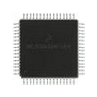
MC68HC705X32CFU Freescale Semiconductor, MC68HC705X32CFU Datasheet - Page 46

MC68HC705X32CFU
Manufacturer Part Number
MC68HC705X32CFU
Description
Manufacturer
Freescale Semiconductor
Datasheet
1.MC68HC705X32CFU.pdf
(232 pages)
Specifications of MC68HC705X32CFU
Cpu Family
HC05
Device Core Size
8b
Frequency (max)
4MHz
Interface Type
SCI
Program Memory Type
EPROM
Program Memory Size
32KB
Total Internal Ram Size
528Byte
# I/os (max)
32
Number Of Timers - General Purpose
1
Operating Supply Voltage (typ)
5V
Operating Supply Voltage (max)
5.5V
Operating Supply Voltage (min)
4.5V
On-chip Adc
8-chx8-bit
Instruction Set Architecture
CISC
Operating Temp Range
-40C to 85C
Operating Temperature Classification
Industrial
Mounting
Surface Mount
Pin Count
64
Package Type
PQFP
Lead Free Status / Rohs Status
Supplier Unconfirmed
Available stocks
Company
Part Number
Manufacturer
Quantity
Price
Part Number:
MC68HC705X32CFU4
Manufacturer:
FREESCALE
Quantity:
20 000
- Current page: 46 of 232
- Download datasheet (6Mb)
3
3.5
The user EEPROM consists of 256 bytes of memory located from address $0100 to $01FF. 255
bytes are general purpose and 1 byte is used by the option register. The non-volatile EEPROM is
byte erasable.
An internal charge pump provides the EEPROM voltage (V
a high voltage for erase and programming functions. The charge pump is a capacitor/diode ladder
network which will give a very high impedance output of around 20-30 M . The voltage of the
charge pump is visible at the VPP1 pin. During normal operation of the device, where
programming/erasing of the EEPROM array will occur, VPP1 should never be connected to either
VDD or VSS as this could prevent the charge pump reaching the necessary programming voltage.
Where it is considered dangerous to leave VPP1 unconnected for reasons of excessive noise in a
system, it may be tied to V
consumption, and therefore it is recommended that the protect bit function is used for regular
protection of EEPROM data (see
In order to achieve a higher degree of security for stored data, there is no capability for bulk or row
erase operations.
The EEPROM control register ($0007) provides control of the EEPROM programming and erase
operations.
Warning: The VPP1 pin should never be connected to VSS, as this could cause permanent
3.5.1
WOIE — Wired-OR interrupt enable
This bit is used to enable wired-OR interrupts on the NWOI pin and on all port B pins which have
been programmed as inputs. Wired-OR interrupts can only be enabled if the WOI mask option is
selected (see
reset clears the WOIE bit.
EEPROM/ECLK control
1 (set)
0 (clear) –
damage to the device.
EEPROM
EEPROM control register
Section
–
Freescale Semiconductor, Inc.
have been selected as a mask option).
Wired-OR interrupts are enabled (provided that wired-OR interrupts
Wired-OR interrupts are disabled.
1.2). WOIE is forced to zero if this mask option is not selected. Power-on
For More Information On This Product,
DD
Address
$0007
; this will protect the EEPROM data but will also increase power
Section
MEMORY AND REGISTERS
Go to: www.freescale.com
WOIE
bit 7
3.5.5).
bit 6
CAF
bit 5
0
bit 4
PP1
0
), which removes the need to supply
ECLK E1ERA E1LAT E1PGM 0000 0000
bit 3
bit 2
bit 1
MC68HC05X16
bit 0
on reset
State
Rev. 1
Related parts for MC68HC705X32CFU
Image
Part Number
Description
Manufacturer
Datasheet
Request
R
Part Number:
Description:
Manufacturer:
Freescale Semiconductor, Inc
Datasheet:
Part Number:
Description:
Manufacturer:
Freescale Semiconductor, Inc
Datasheet:
Part Number:
Description:
Manufacturer:
Freescale Semiconductor, Inc
Datasheet:
Part Number:
Description:
Manufacturer:
Freescale Semiconductor, Inc
Datasheet:
Part Number:
Description:
Manufacturer:
Freescale Semiconductor, Inc
Datasheet:
Part Number:
Description:
Manufacturer:
Freescale Semiconductor, Inc
Datasheet:
Part Number:
Description:
Manufacturer:
Freescale Semiconductor, Inc
Datasheet:
Part Number:
Description:
Manufacturer:
Freescale Semiconductor, Inc
Datasheet:
Part Number:
Description:
Manufacturer:
Freescale Semiconductor, Inc
Datasheet:
Part Number:
Description:
Manufacturer:
Freescale Semiconductor, Inc
Datasheet:
Part Number:
Description:
Manufacturer:
Freescale Semiconductor, Inc
Datasheet:
Part Number:
Description:
Manufacturer:
Freescale Semiconductor, Inc
Datasheet:
Part Number:
Description:
Manufacturer:
Freescale Semiconductor, Inc
Datasheet:
Part Number:
Description:
Manufacturer:
Freescale Semiconductor, Inc
Datasheet:
Part Number:
Description:
Manufacturer:
Freescale Semiconductor, Inc
Datasheet:


