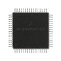
MC68HC705X32CFU Freescale Semiconductor, MC68HC705X32CFU Datasheet - Page 152

MC68HC705X32CFU
Manufacturer Part Number
MC68HC705X32CFU
Description
Manufacturer
Freescale Semiconductor
Datasheet
1.MC68HC705X32CFU.pdf
(232 pages)
Specifications of MC68HC705X32CFU
Cpu Family
HC05
Device Core Size
8b
Frequency (max)
4MHz
Interface Type
SCI
Program Memory Type
EPROM
Program Memory Size
32KB
Total Internal Ram Size
528Byte
# I/os (max)
32
Number Of Timers - General Purpose
1
Operating Supply Voltage (typ)
5V
Operating Supply Voltage (max)
5.5V
Operating Supply Voltage (min)
4.5V
On-chip Adc
8-chx8-bit
Instruction Set Architecture
CISC
Operating Temp Range
-40C to 85C
Operating Temperature Classification
Industrial
Mounting
Surface Mount
Pin Count
64
Package Type
PQFP
Lead Free Status / Rohs Status
Supplier Unconfirmed
Available stocks
Company
Part Number
Manufacturer
Quantity
Price
Part Number:
MC68HC705X32CFU4
Manufacturer:
FREESCALE
Quantity:
20 000
- Current page: 152 of 232
- Download datasheet (6Mb)
11
11.2.1
Most of these instructions use two operands. The first operand is either the accumulator or the
index register. The second operand is obtained from memory using one of the addressing modes.
The jump unconditional (JMP) and jump to subroutine (JSR) instructions have no register operand.
Refer to
11.2.2
These instructions cause the program to branch if a particular condition is met; otherwise, no
operation is performed. Branch instructions are two-byte instructions. Refer to
11.2.3
The MCU can set or clear any writable bit that resides in the first 256 bytes of the memory space
(page 0). All port data and data direction registers, timer and serial interface registers,
control/status registers and a portion of the on-chip RAM reside in page 0. An additional feature
allows the software to test and branch on the state of any bit within these locations. The bit set, bit
clear, bit test and branch functions are all implemented with single instructions. For the test and
branch instructions, the value of the bit tested is also placed in the carry bit of the condition code
register. Refer to
11.2.4
These instructions read a memory location or a register, modify or test its contents, and write the
modified value back to memory or to the register. The test for negative or zero (TST) instruction is
an exception to this sequence of reading, modifying and writing, since it does not modify the value.
Refer to
11.2.5
These instructions are register reference instructions and are used to control processor operation
during program execution. Refer to
11.2.6
Tables for all the instruction types listed above follow. In addition there is a complete alphabetical
listing of all the instructions (see
M68HC05 MCU family (see
Table 11-2
Table 11-5
Register/memory Instructions
Branch instructions
Bit manipulation instructions
Read/modify/write instructions
Control instructions
Tables
Table
Freescale Semiconductor, Inc.
for a complete list of register/memory instructions.
for a complete list of read/modify/write instructions.
11-4.
For More Information On This Product,
Table
CPU CORE AND INSTRUCTION SET
Go to: www.freescale.com
Table
11-8).
Table 11-6
11-7), and an opcode map for the instruction set of the
for a complete list of control instructions.
Table
MC68HC05X16
11-3.
Rev. 1
Related parts for MC68HC705X32CFU
Image
Part Number
Description
Manufacturer
Datasheet
Request
R
Part Number:
Description:
Manufacturer:
Freescale Semiconductor, Inc
Datasheet:
Part Number:
Description:
Manufacturer:
Freescale Semiconductor, Inc
Datasheet:
Part Number:
Description:
Manufacturer:
Freescale Semiconductor, Inc
Datasheet:
Part Number:
Description:
Manufacturer:
Freescale Semiconductor, Inc
Datasheet:
Part Number:
Description:
Manufacturer:
Freescale Semiconductor, Inc
Datasheet:
Part Number:
Description:
Manufacturer:
Freescale Semiconductor, Inc
Datasheet:
Part Number:
Description:
Manufacturer:
Freescale Semiconductor, Inc
Datasheet:
Part Number:
Description:
Manufacturer:
Freescale Semiconductor, Inc
Datasheet:
Part Number:
Description:
Manufacturer:
Freescale Semiconductor, Inc
Datasheet:
Part Number:
Description:
Manufacturer:
Freescale Semiconductor, Inc
Datasheet:
Part Number:
Description:
Manufacturer:
Freescale Semiconductor, Inc
Datasheet:
Part Number:
Description:
Manufacturer:
Freescale Semiconductor, Inc
Datasheet:
Part Number:
Description:
Manufacturer:
Freescale Semiconductor, Inc
Datasheet:
Part Number:
Description:
Manufacturer:
Freescale Semiconductor, Inc
Datasheet:
Part Number:
Description:
Manufacturer:
Freescale Semiconductor, Inc
Datasheet:


