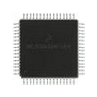
MC68HC705X32CFU Freescale Semiconductor, MC68HC705X32CFU Datasheet - Page 17

MC68HC705X32CFU
Manufacturer Part Number
MC68HC705X32CFU
Description
Manufacturer
Freescale Semiconductor
Datasheet
1.MC68HC705X32CFU.pdf
(232 pages)
Specifications of MC68HC705X32CFU
Cpu Family
HC05
Device Core Size
8b
Frequency (max)
4MHz
Interface Type
SCI
Program Memory Type
EPROM
Program Memory Size
32KB
Total Internal Ram Size
528Byte
# I/os (max)
32
Number Of Timers - General Purpose
1
Operating Supply Voltage (typ)
5V
Operating Supply Voltage (max)
5.5V
Operating Supply Voltage (min)
4.5V
On-chip Adc
8-chx8-bit
Instruction Set Architecture
CISC
Operating Temp Range
-40C to 85C
Operating Temperature Classification
Industrial
Mounting
Surface Mount
Pin Count
64
Package Type
PQFP
Lead Free Status / Rohs Status
Supplier Unconfirmed
Available stocks
Company
Part Number
Manufacturer
Quantity
Price
Part Number:
MC68HC705X32CFU4
Manufacturer:
FREESCALE
Quantity:
20 000
- Current page: 17 of 232
- Download datasheet (6Mb)
Figure
Number
MC68HC05X16
1-1
2-1
2-2
2-3
2-4
2-5
2-6
2-7
3-1
3-2
4-1
4-2
4-3
5-1
5-2
5-3
5-4
5-5
5-6
6-1
6-2
6-3
6-4
6-5
7-1
7-2
7-3
7-4
7-5
7-6
7-7
7-8
7-9
MC68HC05X16 block diagram ............................................................................... 1-4
Bootstrap mode function selection flow chart......................................................... 2-2
MC68HC05X16 ‘jump to any address’ schematic diagram..................................... 2-4
MC68HC05X16 ‘load program in RAM and execute’ schematic diagram............... 2-5
STOP and WAIT flow charts................................................................................... 2-9
Slow mode divider block diagram ........................................................................... 2-10
Oscillator connections ............................................................................................ 2-14
Oscillator divider block diagram.............................................................................. 2-15
Memory map of the MC68HC05X16 ...................................................................... 3-2
MCAN module memory map .................................................................................. 3-3
Standard I/O port structure..................................................................................... 4-2
ECLK timing diagram ............................................................................................. 4-3
Port logic levels ...................................................................................................... 4-7
MCAN block diagram.............................................................................................. 5-1
MCAN frame formats.............................................................................................. 5-2
MCAN module memory map .................................................................................. 5-5
Oscillator block diagram ......................................................................................... 5-15
Segments within the bit time .................................................................................. 5-16
A typical physical interface between the MCAN and the MCAN bus lines ............. 5-23
16-bit programmable timer block diagram .............................................................. 6-2
Timer state timing diagram for reset....................................................................... 6-13
Timer state timing diagram for input capture .......................................................... 6-13
Timer state timing diagram for output compare...................................................... 6-14
Timer state timing diagram for timer overflow......................................................... 6-14
Serial communications interface block diagram ..................................................... 7-2
SCI rate generator division ..................................................................................... 7-4
Data format............................................................................................................. 7-5
SCI examples of start bit sampling technique ........................................................ 7-7
SCI sampling technique used on all bits ................................................................ 7-7
Artificial start following a framing error ................................................................... 7-8
SCI start bit following a break................................................................................. 7-8
SCI example of synchronous and asynchronous transmission .............................. 7-9
SCI data clock timing diagram (M=0) ..................................................................... 7-12
Freescale Semiconductor, Inc.
For More Information On This Product,
LIST OF FIGURES
Go to: www.freescale.com
LIST OF FIGURES
TITLE
Number
Page
ix
Related parts for MC68HC705X32CFU
Image
Part Number
Description
Manufacturer
Datasheet
Request
R
Part Number:
Description:
Manufacturer:
Freescale Semiconductor, Inc
Datasheet:
Part Number:
Description:
Manufacturer:
Freescale Semiconductor, Inc
Datasheet:
Part Number:
Description:
Manufacturer:
Freescale Semiconductor, Inc
Datasheet:
Part Number:
Description:
Manufacturer:
Freescale Semiconductor, Inc
Datasheet:
Part Number:
Description:
Manufacturer:
Freescale Semiconductor, Inc
Datasheet:
Part Number:
Description:
Manufacturer:
Freescale Semiconductor, Inc
Datasheet:
Part Number:
Description:
Manufacturer:
Freescale Semiconductor, Inc
Datasheet:
Part Number:
Description:
Manufacturer:
Freescale Semiconductor, Inc
Datasheet:
Part Number:
Description:
Manufacturer:
Freescale Semiconductor, Inc
Datasheet:
Part Number:
Description:
Manufacturer:
Freescale Semiconductor, Inc
Datasheet:
Part Number:
Description:
Manufacturer:
Freescale Semiconductor, Inc
Datasheet:
Part Number:
Description:
Manufacturer:
Freescale Semiconductor, Inc
Datasheet:
Part Number:
Description:
Manufacturer:
Freescale Semiconductor, Inc
Datasheet:
Part Number:
Description:
Manufacturer:
Freescale Semiconductor, Inc
Datasheet:
Part Number:
Description:
Manufacturer:
Freescale Semiconductor, Inc
Datasheet:


