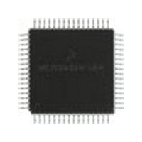
MC68HC705X32CFU Freescale Semiconductor, MC68HC705X32CFU Datasheet - Page 66

MC68HC705X32CFU
Manufacturer Part Number
MC68HC705X32CFU
Description
Manufacturer
Freescale Semiconductor
Datasheet
1.MC68HC705X32CFU.pdf
(232 pages)
Specifications of MC68HC705X32CFU
Cpu Family
HC05
Device Core Size
8b
Frequency (max)
4MHz
Interface Type
SCI
Program Memory Type
EPROM
Program Memory Size
32KB
Total Internal Ram Size
528Byte
# I/os (max)
32
Number Of Timers - General Purpose
1
Operating Supply Voltage (typ)
5V
Operating Supply Voltage (max)
5.5V
Operating Supply Voltage (min)
4.5V
On-chip Adc
8-chx8-bit
Instruction Set Architecture
CISC
Operating Temp Range
-40C to 85C
Operating Temperature Classification
Industrial
Mounting
Surface Mount
Pin Count
64
Package Type
PQFP
Lead Free Status / Rohs Status
Supplier Unconfirmed
Available stocks
Company
Part Number
Manufacturer
Quantity
Price
Part Number:
MC68HC705X32CFU4
Manufacturer:
FREESCALE
Quantity:
20 000
- Current page: 66 of 232
- Download datasheet (6Mb)
5
5.1
The transmit buffer is an interface between the CPU and the bit stream processor (BSP) and is
able to store a complete message. The buffer is written by the CPU and read by the BSP. The CPU
may access this buffer whenever transmit buffer access is set to released. On requesting a
transmission (by setting transmission request in the MCAN command register to present) transmit
buffer access is set to locked, giving the BSP exclusive access to this buffer. The transmit buffer is
released after the message transfer has been completed or aborted.
The TBF is 10 bytes long and holds the identifier (1 byte), the control field (1 byte) and the data
field (maximum length 8 bytes). The buffer is implemented as a single-ported RAM, with mutually
exclusive access by the CPU and the BSP.
5.2
The receive buffer is an interface between the BSP and the CPU and stores a message received
from the bus line. Once filled by the BSP and allocated to the CPU (by the IML), the receive buffer
cannot be used to store subsequent received messages until the CPU has acknowledged the
reading of the buffer’s contents. Thus, unless the CPU releases a receive buffer within a protocol
defined time frame, future messages to be received may be lost.
To reduce the requirements on the CPU, two receive buffers (RBF0 and RBF1) are implemented.
While one receive buffer is allocated to the CPU, the BSP may write to the other buffer. RBF0 and
RBF1 are each 10 bytes long and hold the identifier (1 byte), the control field (1 byte) and the data
field (maximum length 8 bytes). The buffers are implemented as single-ported RAMs with mutually
exclusive access from the CPU and the BSP. The BSP signals the MCU to read the receive buffer
only when the message being received has an identifier that passes the acceptance filter. Note
that a message being transmitted will be automatically written to the receive buffer if the identifier
passes the acceptance filter. This is because it cannot be known, until after the first byte has been
stored, whether or not the transmitting node will lose arbitration to another node.
5.3
The MCAN handles all the communication transactions flowing across the serial bus. For example,
the CPU merely places a message to be transmitted into the transmit buffer and sets the TR bit.
The MCAN will begin transmitting the message when it has determined that the bus is idle. In the
event of a transmission error, the MCAN will initiate a repeated transmission automatically.
TBF – Transmit buffer
RBF – Receive buffer
Interface to the MC68HC05X16 CPU
Freescale Semiconductor, Inc.
For More Information On This Product,
MOTOROLA CAN MODULE (MCAN)
Go to: www.freescale.com
MC68HC05X16
Rev. 1
Related parts for MC68HC705X32CFU
Image
Part Number
Description
Manufacturer
Datasheet
Request
R
Part Number:
Description:
Manufacturer:
Freescale Semiconductor, Inc
Datasheet:
Part Number:
Description:
Manufacturer:
Freescale Semiconductor, Inc
Datasheet:
Part Number:
Description:
Manufacturer:
Freescale Semiconductor, Inc
Datasheet:
Part Number:
Description:
Manufacturer:
Freescale Semiconductor, Inc
Datasheet:
Part Number:
Description:
Manufacturer:
Freescale Semiconductor, Inc
Datasheet:
Part Number:
Description:
Manufacturer:
Freescale Semiconductor, Inc
Datasheet:
Part Number:
Description:
Manufacturer:
Freescale Semiconductor, Inc
Datasheet:
Part Number:
Description:
Manufacturer:
Freescale Semiconductor, Inc
Datasheet:
Part Number:
Description:
Manufacturer:
Freescale Semiconductor, Inc
Datasheet:
Part Number:
Description:
Manufacturer:
Freescale Semiconductor, Inc
Datasheet:
Part Number:
Description:
Manufacturer:
Freescale Semiconductor, Inc
Datasheet:
Part Number:
Description:
Manufacturer:
Freescale Semiconductor, Inc
Datasheet:
Part Number:
Description:
Manufacturer:
Freescale Semiconductor, Inc
Datasheet:
Part Number:
Description:
Manufacturer:
Freescale Semiconductor, Inc
Datasheet:
Part Number:
Description:
Manufacturer:
Freescale Semiconductor, Inc
Datasheet:


