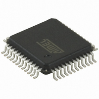
AT32UC3B1128-AUT Atmel, AT32UC3B1128-AUT Datasheet - Page 154

AT32UC3B1128-AUT
Manufacturer Part Number
AT32UC3B1128-AUT
Description
IC MCU AVR32 128KB FLASH 48-TQFP
Manufacturer
Atmel
Series
AVR®32 UC3r
Specifications of AT32UC3B1128-AUT
Core Processor
AVR
Core Size
32-Bit
Speed
60MHz
Connectivity
I²C, IrDA, SPI, SSC, UART/USART, USB
Peripherals
Brown-out Detect/Reset, DMA, POR, PWM, WDT
Number Of I /o
28
Program Memory Size
128KB (128K x 8)
Program Memory Type
FLASH
Ram Size
32K x 8
Voltage - Supply (vcc/vdd)
1.65 V ~ 1.95 V
Data Converters
A/D 6x10b
Oscillator Type
Internal
Operating Temperature
-40°C ~ 85°C
Package / Case
48-TQFP, 48-VQFP
Package
48TQFP
Device Core
AVR32
Family Name
AT32
Maximum Speed
60 MHz
Operating Supply Voltage
1.8|3.3 V
Data Bus Width
32 Bit
Number Of Programmable I/os
28
Interface Type
I2S/SPI/TWI/USART/USB
On-chip Adc
6-chx10-bit
Number Of Timers
3
For Use With
ATSTK600-TQFP48 - STK600 SOCKET/ADAPTER 48-TQFPATAVRONEKIT - KIT AVR/AVR32 DEBUGGER/PROGRMMR770-1008 - ISP 4PORT ATMEL AVR32 MCU SPIATEVK1101 - KIT DEV/EVAL FOR AVR32 AT32UC3B
Lead Free Status / RoHS Status
Lead free / RoHS Compliant
Eeprom Size
-
Available stocks
Company
Part Number
Manufacturer
Quantity
Price
- Current page: 154 of 692
- Download datasheet (11Mb)
16.5
16.5.1
16.5.2
16.5.3
16.5.4
32059K–03/2011
Functional Description
Basic Operation
Memory Pointer
Transfer Counter
Reload Registers
The PDCA consists of multiple independent PDCA channels, each capable of handling DMA
requests in parallel. Each PDCA channels contains a set of configuration registers which must
be configured to start a DMA transfer.
In this section the steps necessary to configure one PDCA channel is outlined.
The peripheral to transfer data to or from must be configured correctly in the Peripheral Select
Register (PSR). This is performed by writing the Peripheral Identity (PID) value for the corre-
sponding peripheral to the PID field in the PSR register. The PID also encodes the transfer
direction, i.e. memory to peripheral or peripheral to memory. See
The transfer size must be written to the Transfer Size field in the Mode Register (MR.SIZE). The
size must match the data size produced or consumed by the selected peripheral. See
16.5.6.
The memory address to transfer to or from, depending on the PSR, must be written to the Mem-
ory Address Register (MAR). For each transfer the memory address is increased by either a
one, two or four, depending on the size set in MR. See
The number of data items to transfer is written to the TCR register. If the PDCA channel is
enabled, a transfer will start immediately after writing a non-zero value to TCR or the reload ver-
sion of TCR, TCRR. After each transfer the TCR value is decreased by one. Both MAR and TCR
can be read while the PDCA channel is active to monitor the DMA progress. See
The channel must be enabled for a transfer to start. A channel is enable by writing a one to the
EN bit in the Control Register (CR).
Each channel has a 32-bit Memory Address Register (MAR). This register holds the memory
address for the next transfer to be performed. The register is automatically updated after each
transfer. The address will be increased by either one, two or four depending on the size of the
DMA transfer (byte, halfword or word). The MAR can be read at any time during transfer.
Each channel has a 16-bit Transfer Counter Register (TCR). This register must be programmed
with the number of transfers to be performed. The TCR register should contain the number of
data items to be transferred independently of the transfer size. The TCR can be read at any time
during transfer to see the number of remaining transfers.
Both the MAR and the TCR have a reload register, respectively Memory Address Reload Regis-
ter (MARR) and Transfer Counter Reload Register (TCRR). These registers provide the
possibility for the PDCA to work on two memory buffers for each channel. When one buffer has
completed, MAR and TCR will be reloaded with the values in MARR and TCRR. The reload logic
is always enabled and will trigger if the TCR reaches zero while TCRR holds a non-zero value.
After reload, the MARR and TCRR registers are cleared.
If TCR is zero when writing to TCRR, the TCR and MAR are automatically updated with the
value written in TCRR and MARR.
Section
16.5.2.
Section
16.5.5.
AT32UC3B
Section
Section
16.5.3.
154
Related parts for AT32UC3B1128-AUT
Image
Part Number
Description
Manufacturer
Datasheet
Request
R

Part Number:
Description:
DEV KIT FOR AVR/AVR32
Manufacturer:
Atmel
Datasheet:

Part Number:
Description:
INTERVAL AND WIPE/WASH WIPER CONTROL IC WITH DELAY
Manufacturer:
ATMEL Corporation
Datasheet:

Part Number:
Description:
Low-Voltage Voice-Switched IC for Hands-Free Operation
Manufacturer:
ATMEL Corporation
Datasheet:

Part Number:
Description:
MONOLITHIC INTEGRATED FEATUREPHONE CIRCUIT
Manufacturer:
ATMEL Corporation
Datasheet:

Part Number:
Description:
AM-FM Receiver IC U4255BM-M
Manufacturer:
ATMEL Corporation
Datasheet:

Part Number:
Description:
Monolithic Integrated Feature Phone Circuit
Manufacturer:
ATMEL Corporation
Datasheet:

Part Number:
Description:
Multistandard Video-IF and Quasi Parallel Sound Processing
Manufacturer:
ATMEL Corporation
Datasheet:

Part Number:
Description:
High-performance EE PLD
Manufacturer:
ATMEL Corporation
Datasheet:

Part Number:
Description:
8-bit Flash Microcontroller
Manufacturer:
ATMEL Corporation
Datasheet:

Part Number:
Description:
2-Wire Serial EEPROM
Manufacturer:
ATMEL Corporation
Datasheet:


