AT32UC3B1128-AUT Atmel, AT32UC3B1128-AUT Datasheet - Page 597
AT32UC3B1128-AUT
Manufacturer Part Number
AT32UC3B1128-AUT
Description
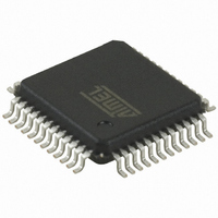
IC MCU AVR32 128KB FLASH 48-TQFP
Manufacturer
Atmel
Series
AVR®32 UC3r
Specifications of AT32UC3B1128-AUT
Core Processor
AVR
Core Size
32-Bit
Speed
60MHz
Connectivity
I²C, IrDA, SPI, SSC, UART/USART, USB
Peripherals
Brown-out Detect/Reset, DMA, POR, PWM, WDT
Number Of I /o
28
Program Memory Size
128KB (128K x 8)
Program Memory Type
FLASH
Ram Size
32K x 8
Voltage - Supply (vcc/vdd)
1.65 V ~ 1.95 V
Data Converters
A/D 6x10b
Oscillator Type
Internal
Operating Temperature
-40°C ~ 85°C
Package / Case
48-TQFP, 48-VQFP
Package
48TQFP
Device Core
AVR32
Family Name
AT32
Maximum Speed
60 MHz
Operating Supply Voltage
1.8|3.3 V
Data Bus Width
32 Bit
Number Of Programmable I/os
28
Interface Type
I2S/SPI/TWI/USART/USB
On-chip Adc
6-chx10-bit
Number Of Timers
3
For Use With
ATSTK600-TQFP48 - STK600 SOCKET/ADAPTER 48-TQFPATAVRONEKIT - KIT AVR/AVR32 DEBUGGER/PROGRMMR770-1008 - ISP 4PORT ATMEL AVR32 MCU SPIATEVK1101 - KIT DEV/EVAL FOR AVR32 AT32UC3B
Lead Free Status / RoHS Status
Lead free / RoHS Compliant
Eeprom Size
-
Available stocks
Company
Part Number
Manufacturer
Quantity
Price


27.4.10
27.4.11
32059K–03/2011
Boundary-scan
Service Access Bus
Apply the TMS sequence 1, 1, 0 to re-enter the Run-Test/Idle state. If the selected Data Register
has a latched parallel-output, the latching takes place in the Update-DR state. The Exit-DR,
Pause-DR, and Exit2-DR states are only used for navigating the state machine.
As shown in the state diagram, the Run-Test/Idle state need not be entered between selecting
JTAG instruction and using Data Registers.
The boundary-scan chain has the capability of driving and observing the logic levels on the digi-
tal I/O pins, as well as the boundary between digital and analog logic for analog circuitry having
off-chip connections. At system level, all ICs having JTAG capabilities are connected serially by
the TDI/TDO signals to form a long shift register. An external controller sets up the devices to
drive values at their output pins, and observe the input values received from other devices. The
controller compares the received data with the expected result. In this way, boundary-scan pro-
vides a mechanism for testing interconnections and integrity of components on Printed Circuits
Boards by using the 4 TAP signals only.
The four IEEE 1149.1 defined mandatory JTAG instructions IDCODE, BYPASS, SAMPLE/PRE-
LOAD, and EXTEST can be used for testing the Printed Circuit Board. Initial scanning of the
data register path will show the ID-code of the device, since IDCODE is the default JTAG
instruction. It may be desirable to have the 32-bit AVR device in reset during test mode. If not
reset, inputs to the device may be determined by the scan operations, and the internal software
may be in an undetermined state when exiting the test mode. If needed, the BYPASS instruction
can be issued to make the shortest possible scan chain through the device. The device can be
set in the reset state either by pulling the external RESETn pin low, or issuing the AVR_RESET
instruction with appropriate setting of the Reset Data Register.
The EXTEST instruction is used for sampling external pins and loading output pins with data.
The data from the output latch will be driven out on the pins as soon as the EXTEST instruction
is loaded into the JTAG IR-register. Therefore, the SAMPLE/PRELOAD should also be used for
setting initial values to the scan ring, to avoid damaging the board when issuing the EXTEST
instruction for the first time. SAMPLE/PRELOAD can also be used for taking a snapshot of the
external pins during normal operation of the part.
When using the JTAG Interface for boundary-scan, the JTAG TCK clock is independent of the
internal chip clock. The internal chip clock is not required to run during boundary-scan
operations.
NOTE: For pins connected to 5V lines care should be taken to not drive the pins to a logic one
using boundary-scan, as this will create a current flowing from the 3,3V driver to the 5V pull-up
on the line. Optionally a series resistor can be added between the line and the pin to reduce the
current.
Details about the boundary-scan chain can be found in the BSDL file for the device. This can be
found on the Atmel website.
The AVR32 architecture offers a common interface for access to On-Chip Debug, programming,
and test functions. These are mapped on a common bus called the Service Access Bus (SAB),
which is linked to the JTAG through a bus master module, which also handles synchronization
between the TCK and SAB clocks.
AT32UC3B
597
Related parts for AT32UC3B1128-AUT
Image
Part Number
Description
Manufacturer
Datasheet
Request
R

Part Number:
Description:
DEV KIT FOR AVR/AVR32
Manufacturer:
Atmel
Datasheet:

Part Number:
Description:
INTERVAL AND WIPE/WASH WIPER CONTROL IC WITH DELAY
Manufacturer:
ATMEL Corporation
Datasheet:
Part Number:
Description:
Low-Voltage Voice-Switched IC for Hands-Free Operation
Manufacturer:
ATMEL Corporation
Datasheet:
Part Number:
Description:
MONOLITHIC INTEGRATED FEATUREPHONE CIRCUIT
Manufacturer:
ATMEL Corporation
Datasheet:
Part Number:
Description:
AM-FM Receiver IC U4255BM-M
Manufacturer:
ATMEL Corporation
Datasheet:
Part Number:
Description:
Monolithic Integrated Feature Phone Circuit
Manufacturer:
ATMEL Corporation
Datasheet:
Part Number:
Description:
Multistandard Video-IF and Quasi Parallel Sound Processing
Manufacturer:
ATMEL Corporation
Datasheet:
Part Number:
Description:
High-performance EE PLD
Manufacturer:
ATMEL Corporation
Datasheet:
Part Number:
Description:
8-bit Flash Microcontroller
Manufacturer:
ATMEL Corporation
Datasheet:
Part Number:
Description:
2-Wire Serial EEPROM
Manufacturer:
ATMEL Corporation
Datasheet: