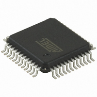
AT32UC3B1128-AUT Atmel, AT32UC3B1128-AUT Datasheet - Page 600

AT32UC3B1128-AUT
Manufacturer Part Number
AT32UC3B1128-AUT
Description
IC MCU AVR32 128KB FLASH 48-TQFP
Manufacturer
Atmel
Series
AVR®32 UC3r
Specifications of AT32UC3B1128-AUT
Core Processor
AVR
Core Size
32-Bit
Speed
60MHz
Connectivity
I²C, IrDA, SPI, SSC, UART/USART, USB
Peripherals
Brown-out Detect/Reset, DMA, POR, PWM, WDT
Number Of I /o
28
Program Memory Size
128KB (128K x 8)
Program Memory Type
FLASH
Ram Size
32K x 8
Voltage - Supply (vcc/vdd)
1.65 V ~ 1.95 V
Data Converters
A/D 6x10b
Oscillator Type
Internal
Operating Temperature
-40°C ~ 85°C
Package / Case
48-TQFP, 48-VQFP
Package
48TQFP
Device Core
AVR32
Family Name
AT32
Maximum Speed
60 MHz
Operating Supply Voltage
1.8|3.3 V
Data Bus Width
32 Bit
Number Of Programmable I/os
28
Interface Type
I2S/SPI/TWI/USART/USB
On-chip Adc
6-chx10-bit
Number Of Timers
3
For Use With
ATSTK600-TQFP48 - STK600 SOCKET/ADAPTER 48-TQFPATAVRONEKIT - KIT AVR/AVR32 DEBUGGER/PROGRMMR770-1008 - ISP 4PORT ATMEL AVR32 MCU SPIATEVK1101 - KIT DEV/EVAL FOR AVR32 AT32UC3B
Lead Free Status / RoHS Status
Lead free / RoHS Compliant
Eeprom Size
-
Available stocks
Company
Part Number
Manufacturer
Quantity
Price
- Current page: 600 of 692
- Download datasheet (11Mb)
27.5
Table 27-7.
27.5.1
32059K–03/2011
Instruction
OPCODE
Others
0x0C
0x0F
0x1C
0x1F
0x01
0x02
0x03
0x04
0x06
0x10
0x11
0x12
0x13
0x14
0x15
0x17
JTAG Instruction Summary
Security Restrictions
JTAG Instruction Summary
SAMPLE_PRELOAD
EXTEST
CLAMP
AVR_RESET
CHIP_ERASE
NEXUS_ACCESS
MEMORY_WORD_ACCESS
MEMORY_SERVICE
MEMORY_SIZED_ACCESS
SYNC
HALT
N/A
Instruction
IDCODE
INTEST
MEMORY_BLOCK_ACCESS
CANCEL_ACCESS
BYPASS
The implemented JTAG instructions in the 32-bit AVR are shown in the table below.
When the security fuse in the Flash is programmed, the following JTAG instructions are
restricted:
For description of what memory locations remain accessible, please refer to the SAB address
map.
Full access to these instructions is re-enabled when the security fuse is erased by the
CHIP_ERASE JTAG instruction.
Note that the security bit will read as programmed and block these instructions also if the Flash
Controller is statically reset.
• NEXUS_ACCESS
• MEMORY_WORD_ACCESS
• MEMORY_BLOCK_ACCESS
• MEMORY_SIZED_ACCESS
Description
Select the 32-bit Device Identification register as data register.
Take a snapshot of external pin values without affecting system operation.
Select boundary-scan chain as data register for testing circuitry external to
the device.
Select boundary-scan chain for internal testing of the device.
Bypass device through Bypass register, while driving outputs from boundary-
scan register.
Apply or remove a static reset to the device
Erase the device
Select the SAB Address and Data registers as data register for the TAP. The
registers are accessed in Nexus mode.
Select the SAB Address and Data registers as data register for the TAP.
Select the SAB Data register as data register for the TAP. The address is
auto-incremented.
Cancel an ongoing Nexus or Memory access.
Select the SAB Address and Data registers as data register for the TAP. The
registers are accessed in Memory Service mode.
Select the SAB Address and Data registers as data register for the TAP.
Synchronization counter
Halt the CPU for safe programming.
Bypass this device through the bypass register.
Acts as BYPASS
AT32UC3B
600
Related parts for AT32UC3B1128-AUT
Image
Part Number
Description
Manufacturer
Datasheet
Request
R

Part Number:
Description:
DEV KIT FOR AVR/AVR32
Manufacturer:
Atmel
Datasheet:

Part Number:
Description:
INTERVAL AND WIPE/WASH WIPER CONTROL IC WITH DELAY
Manufacturer:
ATMEL Corporation
Datasheet:

Part Number:
Description:
Low-Voltage Voice-Switched IC for Hands-Free Operation
Manufacturer:
ATMEL Corporation
Datasheet:

Part Number:
Description:
MONOLITHIC INTEGRATED FEATUREPHONE CIRCUIT
Manufacturer:
ATMEL Corporation
Datasheet:

Part Number:
Description:
AM-FM Receiver IC U4255BM-M
Manufacturer:
ATMEL Corporation
Datasheet:

Part Number:
Description:
Monolithic Integrated Feature Phone Circuit
Manufacturer:
ATMEL Corporation
Datasheet:

Part Number:
Description:
Multistandard Video-IF and Quasi Parallel Sound Processing
Manufacturer:
ATMEL Corporation
Datasheet:

Part Number:
Description:
High-performance EE PLD
Manufacturer:
ATMEL Corporation
Datasheet:

Part Number:
Description:
8-bit Flash Microcontroller
Manufacturer:
ATMEL Corporation
Datasheet:

Part Number:
Description:
2-Wire Serial EEPROM
Manufacturer:
ATMEL Corporation
Datasheet:


