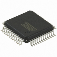
AT32UC3B1128-AUT Atmel, AT32UC3B1128-AUT Datasheet - Page 173

AT32UC3B1128-AUT
Manufacturer Part Number
AT32UC3B1128-AUT
Description
IC MCU AVR32 128KB FLASH 48-TQFP
Manufacturer
Atmel
Series
AVR®32 UC3r
Specifications of AT32UC3B1128-AUT
Core Processor
AVR
Core Size
32-Bit
Speed
60MHz
Connectivity
I²C, IrDA, SPI, SSC, UART/USART, USB
Peripherals
Brown-out Detect/Reset, DMA, POR, PWM, WDT
Number Of I /o
28
Program Memory Size
128KB (128K x 8)
Program Memory Type
FLASH
Ram Size
32K x 8
Voltage - Supply (vcc/vdd)
1.65 V ~ 1.95 V
Data Converters
A/D 6x10b
Oscillator Type
Internal
Operating Temperature
-40°C ~ 85°C
Package / Case
48-TQFP, 48-VQFP
Package
48TQFP
Device Core
AVR32
Family Name
AT32
Maximum Speed
60 MHz
Operating Supply Voltage
1.8|3.3 V
Data Bus Width
32 Bit
Number Of Programmable I/os
28
Interface Type
I2S/SPI/TWI/USART/USB
On-chip Adc
6-chx10-bit
Number Of Timers
3
For Use With
ATSTK600-TQFP48 - STK600 SOCKET/ADAPTER 48-TQFPATAVRONEKIT - KIT AVR/AVR32 DEBUGGER/PROGRMMR770-1008 - ISP 4PORT ATMEL AVR32 MCU SPIATEVK1101 - KIT DEV/EVAL FOR AVR32 AT32UC3B
Lead Free Status / RoHS Status
Lead free / RoHS Compliant
Eeprom Size
-
Available stocks
Company
Part Number
Manufacturer
Quantity
Price
- Current page: 173 of 692
- Download datasheet (11Mb)
17.5.1
17.5.1.1
17.5.1.2
17.5.1.3
32059K–03/2011
Basic Operation
I/O Line or peripheral function selection
Peripheral selection
Output control
Figure 17-2. Overview of the GPIO Pad Connections
When a pin is multiplexed with one or more peripheral functions, the selection is controlled with
the GPIO Enable Register (GPER). If a bit in GPER is written to one, the corresponding pin is
controlled by the GPIO. If a bit is written to zero, the corresponding pin is controlled by a periph-
eral function.
The GPIO provides multiplexing of up to four peripheral functions on a single pin. The selection
is performed by accessing Peripheral Mux Register 0 (PMR0) and Peripheral Mux Register 1
(PMR1).
When the I/O line is assigned to a peripheral function, i.e. the corresponding bit in GPER is writ-
ten to zero, the drive of the I/O line is controlled by the peripheral. The peripheral, depending on
the value in PMR0 and PMR1, determines whether the pin is driven or not.
When the I/O line is controlled by the GPIO, the value of the Output Driver Enable Register
(ODER) determines if the pin is driven or not. When a bit in this register is written to one, the cor-
Periph. C output enable
Periph. D output enable
Periph. A output enable
Periph. B output enable
Periph. A output data
Periph. B output data
Periph. C output data
Periph. D output data
Periph. A input data
Periph. B input data
Periph. C input data
Periph. D input data
PMR1
PMR0
ODER
OVR
GPER
Glitch Filter
PVR
GFER
1
0
0
1
0
1
Edge Detector
IMR1
IMR0
IER
1
0
PUER
AT32UC3B
Interrupt Request
PAD
173
Related parts for AT32UC3B1128-AUT
Image
Part Number
Description
Manufacturer
Datasheet
Request
R

Part Number:
Description:
DEV KIT FOR AVR/AVR32
Manufacturer:
Atmel
Datasheet:

Part Number:
Description:
INTERVAL AND WIPE/WASH WIPER CONTROL IC WITH DELAY
Manufacturer:
ATMEL Corporation
Datasheet:

Part Number:
Description:
Low-Voltage Voice-Switched IC for Hands-Free Operation
Manufacturer:
ATMEL Corporation
Datasheet:

Part Number:
Description:
MONOLITHIC INTEGRATED FEATUREPHONE CIRCUIT
Manufacturer:
ATMEL Corporation
Datasheet:

Part Number:
Description:
AM-FM Receiver IC U4255BM-M
Manufacturer:
ATMEL Corporation
Datasheet:

Part Number:
Description:
Monolithic Integrated Feature Phone Circuit
Manufacturer:
ATMEL Corporation
Datasheet:

Part Number:
Description:
Multistandard Video-IF and Quasi Parallel Sound Processing
Manufacturer:
ATMEL Corporation
Datasheet:

Part Number:
Description:
High-performance EE PLD
Manufacturer:
ATMEL Corporation
Datasheet:

Part Number:
Description:
8-bit Flash Microcontroller
Manufacturer:
ATMEL Corporation
Datasheet:

Part Number:
Description:
2-Wire Serial EEPROM
Manufacturer:
ATMEL Corporation
Datasheet:


