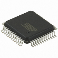
AT32UC3B1128-AUT Atmel, AT32UC3B1128-AUT Datasheet - Page 216

AT32UC3B1128-AUT
Manufacturer Part Number
AT32UC3B1128-AUT
Description
IC MCU AVR32 128KB FLASH 48-TQFP
Manufacturer
Atmel
Series
AVR®32 UC3r
Specifications of AT32UC3B1128-AUT
Core Processor
AVR
Core Size
32-Bit
Speed
60MHz
Connectivity
I²C, IrDA, SPI, SSC, UART/USART, USB
Peripherals
Brown-out Detect/Reset, DMA, POR, PWM, WDT
Number Of I /o
28
Program Memory Size
128KB (128K x 8)
Program Memory Type
FLASH
Ram Size
32K x 8
Voltage - Supply (vcc/vdd)
1.65 V ~ 1.95 V
Data Converters
A/D 6x10b
Oscillator Type
Internal
Operating Temperature
-40°C ~ 85°C
Package / Case
48-TQFP, 48-VQFP
Package
48TQFP
Device Core
AVR32
Family Name
AT32
Maximum Speed
60 MHz
Operating Supply Voltage
1.8|3.3 V
Data Bus Width
32 Bit
Number Of Programmable I/os
28
Interface Type
I2S/SPI/TWI/USART/USB
On-chip Adc
6-chx10-bit
Number Of Timers
3
For Use With
ATSTK600-TQFP48 - STK600 SOCKET/ADAPTER 48-TQFPATAVRONEKIT - KIT AVR/AVR32 DEBUGGER/PROGRMMR770-1008 - ISP 4PORT ATMEL AVR32 MCU SPIATEVK1101 - KIT DEV/EVAL FOR AVR32 AT32UC3B
Lead Free Status / RoHS Status
Lead free / RoHS Compliant
Eeprom Size
-
Available stocks
Company
Part Number
Manufacturer
Quantity
Price
- Current page: 216 of 692
- Download datasheet (11Mb)
18.8.9
Name:
Access Type:
Offset:
Reset Value:
• DLYBCT: Delay Between Consecutive Transfers
• DLYBS: Delay Before SPCK
• ISCBR: Serial Clock Baud Rate
32059K–03/2011
31
23
15
7
This field defines the delay between two consecutive transfers with the same peripheral without removing the chip select. The
delay is always inserted after each transfer and before removing the chip select if needed.
When DLYBCT equals zero, no delay between consecutive transfers is inserted and the clock keeps its duty cycle over the
character transfers.
Otherwise, the following equation determines the delay:
This field defines the delay from NPCS valid to the first valid SPCK transition.
When DLYBS equals zero, the NPCS valid to SPCK transition is 1/2 the SPCK clock period.
Otherwise, the following equations determine the delay:
I
In Master Mode, the SPI Interface uses a modulus counter to derive the SPCK baud rate from the CLK_SPI. The Baud rate is
selected by writing a value from 1 to 255 in the SCBR field. The following equations determine the SPCK baud rate:
Writing 0 to the SCBR field is forbidden. Triggering a transfer while SCBR is 0 can lead to unpredictable results.
At reset, SCBR is 0 and the user has to write it at a valid value before performing the first transfer.
IIf a clock divider (SCBRn) is set to 1 and the other SCBR differ from 1, access on CSn is correct but no correct access will be
possible on others CS.
Delay Between Consecutive Transfers
Delay Before SPCK
SPCK Baudrate
Chip Select Register n
30
22
14
CSRn
Read/Write
0x30 +0x04*n
0x00000000
6
=
BITS
CLKSPI
---------------------
=
SCBR
-------------------- -
CLKSPI
DLYBS
29
21
13
5
=
32
----------------------------------- -
28
20
12
4
CLKSPI
×
DLYBCT
DLYBCT
DLYBS
SCBR
CSAAT
27
19
11
3
CSNAAT
26
18
10
2
NCPHA
25
17
9
1
AT32UC3B
CPOL
24
16
8
0
216
Related parts for AT32UC3B1128-AUT
Image
Part Number
Description
Manufacturer
Datasheet
Request
R

Part Number:
Description:
DEV KIT FOR AVR/AVR32
Manufacturer:
Atmel
Datasheet:

Part Number:
Description:
INTERVAL AND WIPE/WASH WIPER CONTROL IC WITH DELAY
Manufacturer:
ATMEL Corporation
Datasheet:

Part Number:
Description:
Low-Voltage Voice-Switched IC for Hands-Free Operation
Manufacturer:
ATMEL Corporation
Datasheet:

Part Number:
Description:
MONOLITHIC INTEGRATED FEATUREPHONE CIRCUIT
Manufacturer:
ATMEL Corporation
Datasheet:

Part Number:
Description:
AM-FM Receiver IC U4255BM-M
Manufacturer:
ATMEL Corporation
Datasheet:

Part Number:
Description:
Monolithic Integrated Feature Phone Circuit
Manufacturer:
ATMEL Corporation
Datasheet:

Part Number:
Description:
Multistandard Video-IF and Quasi Parallel Sound Processing
Manufacturer:
ATMEL Corporation
Datasheet:

Part Number:
Description:
High-performance EE PLD
Manufacturer:
ATMEL Corporation
Datasheet:

Part Number:
Description:
8-bit Flash Microcontroller
Manufacturer:
ATMEL Corporation
Datasheet:

Part Number:
Description:
2-Wire Serial EEPROM
Manufacturer:
ATMEL Corporation
Datasheet:


