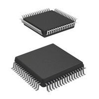
HD64F3664H Renesas Electronics America, HD64F3664H Datasheet - Page 131

HD64F3664H
Manufacturer Part Number
HD64F3664H
Description
IC H8 MCU FLASH 32K 64QFP
Manufacturer
Renesas Electronics America
Series
H8® H8/300H Tinyr
Datasheet
1.US3664-BAG1.pdf
(446 pages)
Specifications of HD64F3664H
Core Processor
H8/300H
Core Size
16-Bit
Speed
16MHz
Connectivity
I²C, SCI
Peripherals
PWM, WDT
Number Of I /o
29
Program Memory Size
32KB (32K x 8)
Program Memory Type
FLASH
Ram Size
2K x 8
Voltage - Supply (vcc/vdd)
3 V ~ 5.5 V
Data Converters
A/D 8x10b
Oscillator Type
External
Operating Temperature
-20°C ~ 75°C
Package / Case
64-QFP
Lead Free Status / RoHS Status
Contains lead / RoHS non-compliant
Eeprom Size
-
Available stocks
Company
Part Number
Manufacturer
Quantity
Price
Company:
Part Number:
HD64F3664H H8/3664
Manufacturer:
RENESAS
Quantity:
13
Company:
Part Number:
HD64F3664HJ
Manufacturer:
TI
Quantity:
171
Part Number:
HD64F3664HJ
Manufacturer:
RENESAS/瑞萨
Quantity:
20 000
Company:
Part Number:
HD64F3664HV
Manufacturer:
ALTERA
Quantity:
101
Company:
Part Number:
HD64F3664HV
Manufacturer:
RENESAS
Quantity:
630
Company:
Part Number:
HD64F3664HV
Manufacturer:
Renesas Electronics America
Quantity:
10 000
Part Number:
HD64F3664HV
Manufacturer:
RENESAS/瑞萨
Quantity:
20 000
- Current page: 131 of 446
- Download datasheet (3Mb)
7.3.1
Table 7.2 shows the boot mode operations between reset end and branching to the programming
control program.
1. When boot mode is used, the flash memory programming control program must be prepared in
2. SCI3 should be set to asynchronous mode, and the transfer format as follows: 8-bit data, 1 stop
3. When the boot program is initiated, the chip measures the low-level period of asynchronous
4. After matching the bit rates, the chip transmits one H'00 byte to the host to indicate the
5. In boot mode, a part of the on-chip RAM area is used by the boot program. The area H'F780 to
6. Before branching to the programming control program, the chip terminates transfer operations
7. Boot mode can be cleared by a reset. End the reset after driving the reset pin low, waiting at
8. Do not change the TEST pin and NMI pin input levels in boot mode.
the host beforehand. Prepare a programming control program in accordance with the
description in section 7.4, Flash Memory Programming/Erasing.
bit, and no parity.
SCI communication data (H'00) transmitted continuously from the host. The chip then
calculates the bit rate of transmission from the host, and adjusts the SCI3 bit rate to match that
of the host. The reset should end with the RxD pin high. The RxD and TxD pins should be
pulled up on the board if necessary. After the reset is complete, it takes approximately 100
states before the chip is ready to measure the low-level period.
completion of bit rate adjustment. The host should confirm that this adjustment end indication
(H'00) has been received normally, and transmit one H'55 byte to the chip. If reception could
not be performed normally, initiate boot mode again by a reset. Depending on the host's
transfer bit rate and system clock frequency of this LSI, there will be a discrepancy between
the bit rates of the host and the chip. To operate the SCI properly, set the host's transfer bit
rate and system clock frequency of this LSI within the ranges listed in table 7.3.
H'FEEF is the area to which the programming control program is transferred from the host.
The boot program area cannot be used until the execution state in boot mode switches to the
programming control program.
by SCI3 (by clearing the RE and TE bits in SCR to 0), however the adjusted bit rate value
remains set in BRR. Therefore, the programming control program can still use it for transfer
of write data or verify data with the host. The TxD pin is high (PCR22 = 1, P22 = 1). The
contents of the CPU general registers are undefined immediately after branching to the
programming control program. These registers must be initialized at the beginning of the
programming control program, as the stack pointer (SP), in particular, is used implicitly in
subroutine calls, etc.
least 20 states, and then setting the TEST pin and NMI pin. Boot mode is also cleared when a
WDT overflow occurs.
Boot Mode
Rev. 6.00 Mar. 24, 2006 Page 101 of 412
REJ09B0142-0600
Section 7 ROM
Related parts for HD64F3664H
Image
Part Number
Description
Manufacturer
Datasheet
Request
R

Part Number:
Description:
(HD64 Series) Hitachi Single-Chip Microcomputer
Manufacturer:
Hitachi Semiconductor
Datasheet:

Part Number:
Description:
KIT STARTER FOR M16C/29
Manufacturer:
Renesas Electronics America
Datasheet:

Part Number:
Description:
KIT STARTER FOR R8C/2D
Manufacturer:
Renesas Electronics America
Datasheet:

Part Number:
Description:
R0K33062P STARTER KIT
Manufacturer:
Renesas Electronics America
Datasheet:

Part Number:
Description:
KIT STARTER FOR R8C/23 E8A
Manufacturer:
Renesas Electronics America
Datasheet:

Part Number:
Description:
KIT STARTER FOR R8C/25
Manufacturer:
Renesas Electronics America
Datasheet:

Part Number:
Description:
KIT STARTER H8S2456 SHARPE DSPLY
Manufacturer:
Renesas Electronics America
Datasheet:

Part Number:
Description:
KIT STARTER FOR R8C38C
Manufacturer:
Renesas Electronics America
Datasheet:

Part Number:
Description:
KIT STARTER FOR R8C35C
Manufacturer:
Renesas Electronics America
Datasheet:

Part Number:
Description:
KIT STARTER FOR R8CL3AC+LCD APPS
Manufacturer:
Renesas Electronics America
Datasheet:

Part Number:
Description:
KIT STARTER FOR RX610
Manufacturer:
Renesas Electronics America
Datasheet:

Part Number:
Description:
KIT STARTER FOR R32C/118
Manufacturer:
Renesas Electronics America
Datasheet:

Part Number:
Description:
KIT DEV RSK-R8C/26-29
Manufacturer:
Renesas Electronics America
Datasheet:

Part Number:
Description:
KIT STARTER FOR SH7124
Manufacturer:
Renesas Electronics America
Datasheet:

Part Number:
Description:
KIT STARTER FOR H8SX/1622
Manufacturer:
Renesas Electronics America
Datasheet:


