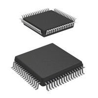
HD64F3664H Renesas Electronics America, HD64F3664H Datasheet - Page 283

HD64F3664H
Manufacturer Part Number
HD64F3664H
Description
IC H8 MCU FLASH 32K 64QFP
Manufacturer
Renesas Electronics America
Series
H8® H8/300H Tinyr
Datasheet
1.US3664-BAG1.pdf
(446 pages)
Specifications of HD64F3664H
Core Processor
H8/300H
Core Size
16-Bit
Speed
16MHz
Connectivity
I²C, SCI
Peripherals
PWM, WDT
Number Of I /o
29
Program Memory Size
32KB (32K x 8)
Program Memory Type
FLASH
Ram Size
2K x 8
Voltage - Supply (vcc/vdd)
3 V ~ 5.5 V
Data Converters
A/D 8x10b
Oscillator Type
External
Operating Temperature
-20°C ~ 75°C
Package / Case
64-QFP
Lead Free Status / RoHS Status
Contains lead / RoHS non-compliant
Eeprom Size
-
Available stocks
Company
Part Number
Manufacturer
Quantity
Price
Company:
Part Number:
HD64F3664H H8/3664
Manufacturer:
RENESAS
Quantity:
13
Company:
Part Number:
HD64F3664HJ
Manufacturer:
TI
Quantity:
171
Part Number:
HD64F3664HJ
Manufacturer:
RENESAS/瑞萨
Quantity:
20 000
Company:
Part Number:
HD64F3664HV
Manufacturer:
ALTERA
Quantity:
101
Company:
Part Number:
HD64F3664HV
Manufacturer:
RENESAS
Quantity:
630
Company:
Part Number:
HD64F3664HV
Manufacturer:
Renesas Electronics America
Quantity:
10 000
Part Number:
HD64F3664HV
Manufacturer:
RENESAS/瑞萨
Quantity:
20 000
- Current page: 283 of 446
- Download datasheet (3Mb)
15.4.3
The data buffer of the I
ICDRS. However, if the completion of receiving the last data is delayed, there will be a contention
between the instruction to issue a stop condition and the SCl clock output to receive the next data,
and may generate unnecessary clocks or fix the output level of the SDA line as low. The switch
timing of the ACKB bit in the ICSR register should be controlled because the acknowledge bit
does not return acknowledgement after receiving the last data in master mode. These problems can
be avoided by using the WAIT function. Follow the flowchart shown below.
In master receive mode, the master device outputs the receive clock, receives data, and returns an
acknowledge signal. The slave device transmits data. The reception procedure and operations with
the wait function synchronized with the ICDR read operation to receive data in sequence are
shown below.
1. Clear the TRS bit in ICCR to 0 to switch from transmit mode to receive mode, and set the
2. When ICDR is read (dummy data read), reception is started, and the receive clock is output,
3. The IRIC flag is set to 1 at the fall of the 8th receive clock pulse. If the IEIC bit in ICCR has
4. Clear the IRIC flag to release from the Wait State. The master device outputs the 9th clock and
5. When one frame of data has been received, the IRIC flag in ICCR and the IRTR flag in ICSR
6. Read ICDR.
7. Clear the IRIC flag to detect next wait operation. Data reception process from the step [5] to
8. The IRIC flags set to 1 at the fall of 8th receive clock pulse. SCL is automatically fixed low in
WAIT bit in ICMR to 1. Also clear the bit in ICSR to ACKB 0 (acknowledge data setting).
and data received, in synchronization with the internal clock. In order to detect wait operation,
set the IRIC flag in ICCR must be cleared to 0. After reading ICDR, clear IRIC continuously
not to execute other interrupt handling routine. If one frame of data has been received before
the IRIC clearing, it can not be determine the end of reception.
been set to 1, an interrupt request is sent to the CPU. SCL is automatically fixed low in
synchronization with the internal clock until the IRIC flag clearing. If the first frame is the last
receive data, execute the step [10] to halt reception.
drives SDA at the 9th receive clock pulse to return an acknowledge signal.
are set to 1 at the rise of the 9th receive clock pulse. The master device outputs SCL clock to
receive next data.
[7] should be executed during one byte reception period after IRIC flag clearing in the step [4]
or [9] to release wait status.
synchronization with the internal clock until the IRIC flag clearing. If this frame is the last
receive data, execute the step [10] to halt reception.
Master Receive Operation
2
C module can receive data consecutively since it consists of ICDRR and
Rev. 6.00 Mar. 24, 2006 Page 253 of 412
Section 15 I
2
C Bus Interface (IIC)
REJ09B0142-0600
Related parts for HD64F3664H
Image
Part Number
Description
Manufacturer
Datasheet
Request
R

Part Number:
Description:
(HD64 Series) Hitachi Single-Chip Microcomputer
Manufacturer:
Hitachi Semiconductor
Datasheet:

Part Number:
Description:
KIT STARTER FOR M16C/29
Manufacturer:
Renesas Electronics America
Datasheet:

Part Number:
Description:
KIT STARTER FOR R8C/2D
Manufacturer:
Renesas Electronics America
Datasheet:

Part Number:
Description:
R0K33062P STARTER KIT
Manufacturer:
Renesas Electronics America
Datasheet:

Part Number:
Description:
KIT STARTER FOR R8C/23 E8A
Manufacturer:
Renesas Electronics America
Datasheet:

Part Number:
Description:
KIT STARTER FOR R8C/25
Manufacturer:
Renesas Electronics America
Datasheet:

Part Number:
Description:
KIT STARTER H8S2456 SHARPE DSPLY
Manufacturer:
Renesas Electronics America
Datasheet:

Part Number:
Description:
KIT STARTER FOR R8C38C
Manufacturer:
Renesas Electronics America
Datasheet:

Part Number:
Description:
KIT STARTER FOR R8C35C
Manufacturer:
Renesas Electronics America
Datasheet:

Part Number:
Description:
KIT STARTER FOR R8CL3AC+LCD APPS
Manufacturer:
Renesas Electronics America
Datasheet:

Part Number:
Description:
KIT STARTER FOR RX610
Manufacturer:
Renesas Electronics America
Datasheet:

Part Number:
Description:
KIT STARTER FOR R32C/118
Manufacturer:
Renesas Electronics America
Datasheet:

Part Number:
Description:
KIT DEV RSK-R8C/26-29
Manufacturer:
Renesas Electronics America
Datasheet:

Part Number:
Description:
KIT STARTER FOR SH7124
Manufacturer:
Renesas Electronics America
Datasheet:

Part Number:
Description:
KIT STARTER FOR H8SX/1622
Manufacturer:
Renesas Electronics America
Datasheet:


