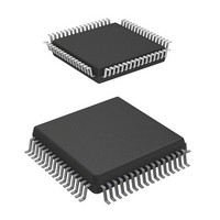
HD64F3664H Renesas Electronics America, HD64F3664H Datasheet - Page 253

HD64F3664H
Manufacturer Part Number
HD64F3664H
Description
IC H8 MCU FLASH 32K 64QFP
Manufacturer
Renesas Electronics America
Series
H8® H8/300H Tinyr
Datasheet
1.US3664-BAG1.pdf
(446 pages)
Specifications of HD64F3664H
Core Processor
H8/300H
Core Size
16-Bit
Speed
16MHz
Connectivity
I²C, SCI
Peripherals
PWM, WDT
Number Of I /o
29
Program Memory Size
32KB (32K x 8)
Program Memory Type
FLASH
Ram Size
2K x 8
Voltage - Supply (vcc/vdd)
3 V ~ 5.5 V
Data Converters
A/D 8x10b
Oscillator Type
External
Operating Temperature
-20°C ~ 75°C
Package / Case
64-QFP
Lead Free Status / RoHS Status
Contains lead / RoHS non-compliant
Eeprom Size
-
Available stocks
Company
Part Number
Manufacturer
Quantity
Price
Company:
Part Number:
HD64F3664H H8/3664
Manufacturer:
RENESAS
Quantity:
13
Company:
Part Number:
HD64F3664HJ
Manufacturer:
TI
Quantity:
171
Part Number:
HD64F3664HJ
Manufacturer:
RENESAS/瑞萨
Quantity:
20 000
Company:
Part Number:
HD64F3664HV
Manufacturer:
ALTERA
Quantity:
101
Company:
Part Number:
HD64F3664HV
Manufacturer:
RENESAS
Quantity:
630
Company:
Part Number:
HD64F3664HV
Manufacturer:
Renesas Electronics America
Quantity:
10 000
Part Number:
HD64F3664HV
Manufacturer:
RENESAS/瑞萨
Quantity:
20 000
- Current page: 253 of 446
- Download datasheet (3Mb)
14.5.5
Figure 14.14 shows a sample flowchart for simultaneous serial transmit and receive operations.
The following procedure should be used for simultaneous serial data transmit and receive
operations. To switch from transmit mode to simultaneous transmit and receive mode, after
checking that the SCI3 has finished transmission and the TDRE and TEND flags are set to 1, clear
TE to 0. Then simultaneously set TE and RE to 1 with a single instruction. To switch from receive
mode to simultaneous transmit and receive mode, after checking that the SCI3 has finished
reception, clear RE to 0. Then after checking that the RDRF and receive error flags (OER, FER,
and PER) are cleared to 0, simultaneously set TE and RE to 1 with a single instruction.
Figure 14.14 Sample Flowchart of Simultaneous Serial Transmit and Receive Operations
Simultaneous Serial Data Transmission and Reception
Yes
No
No
Clear TE and RE bits in SCR to 0
Start transmission/reception
Write transmit data to TDR
Read receive data in RDR
Read RDRF flag in SSR
Read TDRE flag in SSR
Read OER flag in SSR
All data received?
RDRF = 1
TDRE = 1
OER = 1
<End>
Yes
Yes
No
No
(Clocked Synchronous Mode)
Error processing
Yes
[1]
[2]
[3]
[4]
Section 14 Serial Communication Interface 3 (SCI3)
[1] Read SSR and check that the TDRE
[2] Read SSR and check that the RDRF
[3] To continue serial transmission/
[4] If an overrun error occurs, read the
For overrun error processing, see
flag is set to 1, then write transmit
data to TDR.
TDRE flag is automatically cleared
to 0.
flag is set to 1, then read the receive
data in RDR.
RDRF flag is automatically cleared
to 0.
reception, before the MSB (bit 7) of
the current frame is received, finish
reading the RDRF flag, reading
RDR. Also, before the MSB (bit 7)
of the current frame is transmitted,
read 1 from the TDRE flag to confirm
that writing is possible. Then write
data to TDR.
TDRE flag is automatically cleared
to 0. When data is read from RDR,
the RDRF flag is automatically
cleared to 0.
OER flag in SSR, and after
performing the appropriate error
processing, clear the OER flag to 0.
Transmission/reception cannot be
resumed if the OER flag is set to 1.
figure 14.13.
Rev. 6.00 Mar. 24, 2006 Page 223 of 412
When data is written to TDR, the
When data is read from RDR, the
When data is written to TDR, the
REJ09B0142-0600
Related parts for HD64F3664H
Image
Part Number
Description
Manufacturer
Datasheet
Request
R

Part Number:
Description:
(HD64 Series) Hitachi Single-Chip Microcomputer
Manufacturer:
Hitachi Semiconductor
Datasheet:

Part Number:
Description:
KIT STARTER FOR M16C/29
Manufacturer:
Renesas Electronics America
Datasheet:

Part Number:
Description:
KIT STARTER FOR R8C/2D
Manufacturer:
Renesas Electronics America
Datasheet:

Part Number:
Description:
R0K33062P STARTER KIT
Manufacturer:
Renesas Electronics America
Datasheet:

Part Number:
Description:
KIT STARTER FOR R8C/23 E8A
Manufacturer:
Renesas Electronics America
Datasheet:

Part Number:
Description:
KIT STARTER FOR R8C/25
Manufacturer:
Renesas Electronics America
Datasheet:

Part Number:
Description:
KIT STARTER H8S2456 SHARPE DSPLY
Manufacturer:
Renesas Electronics America
Datasheet:

Part Number:
Description:
KIT STARTER FOR R8C38C
Manufacturer:
Renesas Electronics America
Datasheet:

Part Number:
Description:
KIT STARTER FOR R8C35C
Manufacturer:
Renesas Electronics America
Datasheet:

Part Number:
Description:
KIT STARTER FOR R8CL3AC+LCD APPS
Manufacturer:
Renesas Electronics America
Datasheet:

Part Number:
Description:
KIT STARTER FOR RX610
Manufacturer:
Renesas Electronics America
Datasheet:

Part Number:
Description:
KIT STARTER FOR R32C/118
Manufacturer:
Renesas Electronics America
Datasheet:

Part Number:
Description:
KIT DEV RSK-R8C/26-29
Manufacturer:
Renesas Electronics America
Datasheet:

Part Number:
Description:
KIT STARTER FOR SH7124
Manufacturer:
Renesas Electronics America
Datasheet:

Part Number:
Description:
KIT STARTER FOR H8SX/1622
Manufacturer:
Renesas Electronics America
Datasheet:


