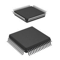
HD64F3664H Renesas Electronics America, HD64F3664H Datasheet - Page 22

HD64F3664H
Manufacturer Part Number
HD64F3664H
Description
IC H8 MCU FLASH 32K 64QFP
Manufacturer
Renesas Electronics America
Series
H8® H8/300H Tinyr
Datasheet
1.US3664-BAG1.pdf
(446 pages)
Specifications of HD64F3664H
Core Processor
H8/300H
Core Size
16-Bit
Speed
16MHz
Connectivity
I²C, SCI
Peripherals
PWM, WDT
Number Of I /o
29
Program Memory Size
32KB (32K x 8)
Program Memory Type
FLASH
Ram Size
2K x 8
Voltage - Supply (vcc/vdd)
3 V ~ 5.5 V
Data Converters
A/D 8x10b
Oscillator Type
External
Operating Temperature
-20°C ~ 75°C
Package / Case
64-QFP
Lead Free Status / RoHS Status
Contains lead / RoHS non-compliant
Eeprom Size
-
Available stocks
Company
Part Number
Manufacturer
Quantity
Price
Company:
Part Number:
HD64F3664H H8/3664
Manufacturer:
RENESAS
Quantity:
13
Company:
Part Number:
HD64F3664HJ
Manufacturer:
TI
Quantity:
171
Part Number:
HD64F3664HJ
Manufacturer:
RENESAS/瑞萨
Quantity:
20 000
Company:
Part Number:
HD64F3664HV
Manufacturer:
ALTERA
Quantity:
101
Company:
Part Number:
HD64F3664HV
Manufacturer:
RENESAS
Quantity:
630
Company:
Part Number:
HD64F3664HV
Manufacturer:
Renesas Electronics America
Quantity:
10 000
Part Number:
HD64F3664HV
Manufacturer:
RENESAS/瑞萨
Quantity:
20 000
- Current page: 22 of 446
- Download datasheet (3Mb)
Figure 4.2 Address Break Interrupt Operation Example (1)......................................................... 71
Figure 4.2 Address Break Interrupt Operation Example (2)......................................................... 72
Figure 4.3 Operation when Condition is not Satisfied in Branch Instruction ............................... 73
Figure 4.4 Operation when Another Interrupt is Accepted at
Figure 4.5 Operation when the Instruction Set is not Executed
Section 5 Clock Pulse Generators
Figure 5.1 Block Diagram of Clock Pulse Generators.................................................................. 77
Figure 5.2 Block Diagram of System Clock Generator ................................................................ 78
Figure 5.3 Typical Connection to Crystal Resonator.................................................................... 78
Figure 5.4 Equivalent Circuit of Crystal Resonator...................................................................... 78
Figure 5.5 Typical Connection to Ceramic Resonator.................................................................. 79
Figure 5.6 Example of External Clock Input ................................................................................ 79
Figure 5.7 Block Diagram of Subclock Generator ....................................................................... 80
Figure 5.8 Typical Connection to 32.768-kHz Crystal Resonator................................................ 80
Figure 5.9 Equivalent Circuit of 32.768-kHz Crystal Resonator.................................................. 80
Figure 5.10 Pin Connection when not Using Subclock ................................................................ 81
Figure 5.11 Example of Incorrect Board Design .......................................................................... 82
Section 6 Power-Down Modes
Figure 6.1 Mode Transition Diagram ........................................................................................... 88
Section 7 ROM
Figure 7.1 Flash Memory Block Configuration............................................................................ 96
Figure 7.2 Programming/Erasing Flowchart Example in User Program Mode.......................... 103
Figure 7.3 Program/Program-Verify Flowchart ......................................................................... 105
Figure 7.4 Erase/Erase-Verify Flowchart ................................................................................... 108
Section 9 I/O Ports
Figure 9.1 Port 1 Pin Configuration............................................................................................ 115
Figure 9.2 Port 2 Pin Configuration............................................................................................ 121
Figure 9.3 Port 5 Pin Configuration............................................................................................ 124
Figure 9.4 Port 7 Pin Configuration............................................................................................ 130
Figure 9.5 Port 8 Pin Configuration............................................................................................ 133
Figure 9.6 Port B Pin Configuration........................................................................................... 138
Section 10 Timer A
Figure 10.1 Block Diagram of Timer A ..................................................................................... 140
Section 11 Timer V
Figure 11.1 Block Diagram of Timer V ..................................................................................... 146
Rev. 6.00 Mar. 24, 2006 Page xx of xxviii
Address Break Setting Instruction ............................................................................... 74
and does not Branch due to Conditions not Being Satisfied ........................................ 75
Related parts for HD64F3664H
Image
Part Number
Description
Manufacturer
Datasheet
Request
R

Part Number:
Description:
(HD64 Series) Hitachi Single-Chip Microcomputer
Manufacturer:
Hitachi Semiconductor
Datasheet:

Part Number:
Description:
KIT STARTER FOR M16C/29
Manufacturer:
Renesas Electronics America
Datasheet:

Part Number:
Description:
KIT STARTER FOR R8C/2D
Manufacturer:
Renesas Electronics America
Datasheet:

Part Number:
Description:
R0K33062P STARTER KIT
Manufacturer:
Renesas Electronics America
Datasheet:

Part Number:
Description:
KIT STARTER FOR R8C/23 E8A
Manufacturer:
Renesas Electronics America
Datasheet:

Part Number:
Description:
KIT STARTER FOR R8C/25
Manufacturer:
Renesas Electronics America
Datasheet:

Part Number:
Description:
KIT STARTER H8S2456 SHARPE DSPLY
Manufacturer:
Renesas Electronics America
Datasheet:

Part Number:
Description:
KIT STARTER FOR R8C38C
Manufacturer:
Renesas Electronics America
Datasheet:

Part Number:
Description:
KIT STARTER FOR R8C35C
Manufacturer:
Renesas Electronics America
Datasheet:

Part Number:
Description:
KIT STARTER FOR R8CL3AC+LCD APPS
Manufacturer:
Renesas Electronics America
Datasheet:

Part Number:
Description:
KIT STARTER FOR RX610
Manufacturer:
Renesas Electronics America
Datasheet:

Part Number:
Description:
KIT STARTER FOR R32C/118
Manufacturer:
Renesas Electronics America
Datasheet:

Part Number:
Description:
KIT DEV RSK-R8C/26-29
Manufacturer:
Renesas Electronics America
Datasheet:

Part Number:
Description:
KIT STARTER FOR SH7124
Manufacturer:
Renesas Electronics America
Datasheet:

Part Number:
Description:
KIT STARTER FOR H8SX/1622
Manufacturer:
Renesas Electronics America
Datasheet:


