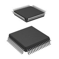
HD64F3664H Renesas Electronics America, HD64F3664H Datasheet - Page 135

HD64F3664H
Manufacturer Part Number
HD64F3664H
Description
IC H8 MCU FLASH 32K 64QFP
Manufacturer
Renesas Electronics America
Series
H8® H8/300H Tinyr
Datasheet
1.US3664-BAG1.pdf
(446 pages)
Specifications of HD64F3664H
Core Processor
H8/300H
Core Size
16-Bit
Speed
16MHz
Connectivity
I²C, SCI
Peripherals
PWM, WDT
Number Of I /o
29
Program Memory Size
32KB (32K x 8)
Program Memory Type
FLASH
Ram Size
2K x 8
Voltage - Supply (vcc/vdd)
3 V ~ 5.5 V
Data Converters
A/D 8x10b
Oscillator Type
External
Operating Temperature
-20°C ~ 75°C
Package / Case
64-QFP
Lead Free Status / RoHS Status
Contains lead / RoHS non-compliant
Eeprom Size
-
Available stocks
Company
Part Number
Manufacturer
Quantity
Price
Company:
Part Number:
HD64F3664H H8/3664
Manufacturer:
RENESAS
Quantity:
13
Company:
Part Number:
HD64F3664HJ
Manufacturer:
TI
Quantity:
171
Part Number:
HD64F3664HJ
Manufacturer:
RENESAS/瑞萨
Quantity:
20 000
Company:
Part Number:
HD64F3664HV
Manufacturer:
ALTERA
Quantity:
101
Company:
Part Number:
HD64F3664HV
Manufacturer:
RENESAS
Quantity:
630
Company:
Part Number:
HD64F3664HV
Manufacturer:
Renesas Electronics America
Quantity:
10 000
Part Number:
HD64F3664HV
Manufacturer:
RENESAS/瑞萨
Quantity:
20 000
- Current page: 135 of 446
- Download datasheet (3Mb)
8. The maximum number of repetitions of the program/program-verify sequence of the same bit
is 1,000.
Note: *The RTS instruction must not be used during the following 1. and 2. periods.
Wait (Wait time=programming time)
1. A period between 128-byte data programming to flash memory and the P bit clearing
2. A period between dummy writing of H'FF to a verify address and verify data reading
Write pulse application subroutine
Clear PSU bit in FLMCR1
Set PSU bit in FLMCR1
Clear P bit in FLMCR1
Set P bit in FLMCR1
Apply Write Pulse
WDT enable
Disable WDT
Wait 50 s
Wait 5 s
Wait 5 s
End Sub
Figure 7.3 Program/Program-Verify Flowchart
*
Increment address
Successively write 128-byte data from additional-
programming data area in RAM to flash memory
No
Additional-programming data computation
Store 128-byte program data in program
data area consecutively to flash memory
Write 128-byte data in RAM reprogram
H'FF dummy write to verify address
data area and reprogram data area
Clear SWE bit in FLMCR1
Set block start address as
Reprogram data computation
data verification completed?
Set SWE bit in FLMCR1
Clear PV bit in FLMCR1
Set PV bit in FLMCR1
Apply Write Pulse
End of programming
Apply
Read verify data
verify address
Yes
Yes
Wait 100 s
Verify data =
write data?
Wait 1 s
Wait 4 s
Wait 2 s
Wait 2 s
Yes
128-byte
START
n 6 ?
m= 0 ?
m= 0
n 6?
n= 1
Write pulse
Yes
Yes
Sub-Routine-Call
No
No
No
Rev. 6.00 Mar. 24, 2006 Page 105 of 412
No
*
m = 1
Clear SWE bit in FLMCR1
Programming failure
Wait 100 s
n
1000 ?
No
Yes
n
REJ09B0142-0600
n + 1
Section 7 ROM
Related parts for HD64F3664H
Image
Part Number
Description
Manufacturer
Datasheet
Request
R

Part Number:
Description:
(HD64 Series) Hitachi Single-Chip Microcomputer
Manufacturer:
Hitachi Semiconductor
Datasheet:

Part Number:
Description:
KIT STARTER FOR M16C/29
Manufacturer:
Renesas Electronics America
Datasheet:

Part Number:
Description:
KIT STARTER FOR R8C/2D
Manufacturer:
Renesas Electronics America
Datasheet:

Part Number:
Description:
R0K33062P STARTER KIT
Manufacturer:
Renesas Electronics America
Datasheet:

Part Number:
Description:
KIT STARTER FOR R8C/23 E8A
Manufacturer:
Renesas Electronics America
Datasheet:

Part Number:
Description:
KIT STARTER FOR R8C/25
Manufacturer:
Renesas Electronics America
Datasheet:

Part Number:
Description:
KIT STARTER H8S2456 SHARPE DSPLY
Manufacturer:
Renesas Electronics America
Datasheet:

Part Number:
Description:
KIT STARTER FOR R8C38C
Manufacturer:
Renesas Electronics America
Datasheet:

Part Number:
Description:
KIT STARTER FOR R8C35C
Manufacturer:
Renesas Electronics America
Datasheet:

Part Number:
Description:
KIT STARTER FOR R8CL3AC+LCD APPS
Manufacturer:
Renesas Electronics America
Datasheet:

Part Number:
Description:
KIT STARTER FOR RX610
Manufacturer:
Renesas Electronics America
Datasheet:

Part Number:
Description:
KIT STARTER FOR R32C/118
Manufacturer:
Renesas Electronics America
Datasheet:

Part Number:
Description:
KIT DEV RSK-R8C/26-29
Manufacturer:
Renesas Electronics America
Datasheet:

Part Number:
Description:
KIT STARTER FOR SH7124
Manufacturer:
Renesas Electronics America
Datasheet:

Part Number:
Description:
KIT STARTER FOR H8SX/1622
Manufacturer:
Renesas Electronics America
Datasheet:


