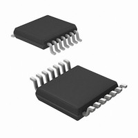
MRF49XA-I/ST Microchip Technology, MRF49XA-I/ST Datasheet - Page 16

MRF49XA-I/ST
Manufacturer Part Number
MRF49XA-I/ST
Description
IC RF TXRX 433/868/915 16-TSSOP
Manufacturer
Microchip Technology
Datasheet
1.MRF49XA-IST.pdf
(102 pages)
Specifications of MRF49XA-I/ST
Package / Case
16-TSSOP
Frequency
433MHz, 868MHz, 915MHz
Data Rate - Maximum
256kbps
Modulation Or Protocol
FHSS, FSK
Applications
Home / Industrial Automation, Remote Access, Security Alarms
Power - Output
7dbm
Sensitivity
-110dBm
Voltage - Supply
2.2 V ~ 3.8 V
Current - Receiving
11mA
Current - Transmitting
15mA
Data Interface
PCB, Surface Mount
Antenna Connector
PCB, Surface Mount
Operating Temperature
-40°C ~ 85°C
Number Of Receivers
1
Number Of Transmitters
2
Wireless Frequency
433 MHz to 915 MHz
Output Power
+ 7 dBm
Operating Supply Voltage
2.5 V, 3.3 V
Maximum Operating Temperature
+ 85 C
Mounting Style
SMD/SMT
Minimum Operating Temperature
- 40 C
Modulation
FHSS, FSK
Lead Free Status / RoHS Status
Lead free / RoHS Compliant
Memory Size
-
Lead Free Status / Rohs Status
Lead free / RoHS Compliant
Other names
579-MRF49XA-1/ST
Available stocks
Company
Part Number
Manufacturer
Quantity
Price
Company:
Part Number:
MRF49XA-I/ST
Manufacturer:
IR
Quantity:
450
Part Number:
MRF49XA-I/ST
Manufacturer:
MICROCHIP/微芯
Quantity:
20 000
referenced with the crystal oscillator. The calibration is
2.11
2.11.1
The integrated low-battery voltage detector circuit
monitors the supply voltage against a preprogrammed
value and generates an interrupt on the IRO pin if it falls
below the programmed threshold level. The detector
circuit has a built-in 50 mV hysteresis.
2.11.2
The current consumption of the programmable wake-up
timer is very low, typically 1.5 μA. It is programmable
from 1 ms to several days with an accuracy level of
±10%. The calibration of the wake-up timer takes place
at every start-up and every 30s thereafter, and is
performed even in Sleep mode. The calibration process
for the wake-up timer takes around 500 μs, and for
proper calibration, the crystal oscillator must be running
before the wake-up timer is enabled.
If any wake-up event occurs, including the wake-up
timer, the wake-up logic generates an interrupt signal
on the IRO pin which can be used to wake-up the
microcontroller and this reduces the period that the
microcontroller needs to be active. If the oscillator
circuit is disabled, the calibration circuit turns it on for a
brief period to perform the calibration in order to
maintain accurate timing before returning to Sleep.
2.11.3
The MRF49XA can be made to enter into a Low Duty
Cycle mode operation to decrease the average power
consumption in Receive mode. The Low Duty Cycle
mode is normally used in conjunction with the wake-up
timer for its operation. The DCSREG may be config-
ured so that when the wake-up timer brings the device
out of Sleep mode, the receiver is turned on for a short
time to sample for a signal. Then, the device returns to
Sleep and this process repeats.
DS70590B-page 14
MRF49XA
Power-Saving Blocks
LOW BATTERY VOLTAGE
DETECTOR
WAKE-UP TIMER
LOW DUTY CYCLE MODE
Preliminary
2.12
The Interrupt pin (INT) can be configured as an
active-low external interrupt to MRF49XA which is
provided from the host microcontroller.
The device generates an interrupt request for the host
microcontroller by pulling the IRO pin low if the
following events occur:
• TX register is ready to receive the next byte
• RX FIFO has received the preprogrammed
• FIFO overflow/TX register underrun (TXUROW
• Negative pulse on interrupt input pin, INT
• Wake-up timer time-out
• Supply voltage below the preprogrammed value is
• Power-on Reset
The Status bits should be read out to identify the source
of interrupt. The interrupts are cleared by reading the
STATUS register.
See Section 3.9 “Interrupts” for functional description
of interrupts.
2.13
The Transmit register in MRF49XA is configured as
two, 8-bit shift registers connected in series to form a
single 16-bit shift register. When the transmitter is
enabled, it starts sending out data from the first register
with respect to the set bit rate. After power-up and with
the Transmit registers enabled, the transmitter pre-
loads the TX latch with 0xAAAA. This can be used to
generate a preamble before sending actual data.
In hardware, the FSK/DATA/FSEL has two functions:
• As Frequency Shift Keying pin, it basically takes
• As DATA (Data Out), this pin receives the data in
amount of bits
overflow in Receive mode and underrun in
Transmit mode)
detected
care of transmitting the FSK data input. The pin
has an internal pull-up resistor of 133 kΩ. This pin
must be “high” when the TX register is enabled to
take care of the transmission.
conjunction with RCLKOUT when the internal
FIFO is not used. When reading the internal
RXFIFOREG, this pin must be pulled “low”.
INT, IRO Pins and Interrupts
Transmit Register
© 2009 Microchip Technology Inc.


