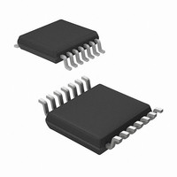
MRF49XA-I/ST Microchip Technology, MRF49XA-I/ST Datasheet - Page 64

MRF49XA-I/ST
Manufacturer Part Number
MRF49XA-I/ST
Description
IC RF TXRX 433/868/915 16-TSSOP
Manufacturer
Microchip Technology
Datasheet
1.MRF49XA-IST.pdf
(102 pages)
Specifications of MRF49XA-I/ST
Package / Case
16-TSSOP
Frequency
433MHz, 868MHz, 915MHz
Data Rate - Maximum
256kbps
Modulation Or Protocol
FHSS, FSK
Applications
Home / Industrial Automation, Remote Access, Security Alarms
Power - Output
7dbm
Sensitivity
-110dBm
Voltage - Supply
2.2 V ~ 3.8 V
Current - Receiving
11mA
Current - Transmitting
15mA
Data Interface
PCB, Surface Mount
Antenna Connector
PCB, Surface Mount
Operating Temperature
-40°C ~ 85°C
Number Of Receivers
1
Number Of Transmitters
2
Wireless Frequency
433 MHz to 915 MHz
Output Power
+ 7 dBm
Operating Supply Voltage
2.5 V, 3.3 V
Maximum Operating Temperature
+ 85 C
Mounting Style
SMD/SMT
Minimum Operating Temperature
- 40 C
Modulation
FHSS, FSK
Lead Free Status / RoHS Status
Lead free / RoHS Compliant
Memory Size
-
Lead Free Status / Rohs Status
Lead free / RoHS Compliant
Other names
579-MRF49XA-1/ST
Available stocks
Company
Part Number
Manufacturer
Quantity
Price
Company:
Part Number:
MRF49XA-I/ST
Manufacturer:
IR
Quantity:
450
Part Number:
MRF49XA-I/ST
Manufacturer:
MICROCHIP/微芯
Quantity:
20 000
3.15
In Low Duty Cycle mode, the receiver periodically
wakes up for a short period and checks for the valid
FSK transmission in progress. The FSK transmission is
detected in the frequency range determined by
CFSREG and the baseband filter bandwidth is deter-
mined by the RXCREG. The on time is automatically
extended until the DQI indicates a good received signal
condition.
The following facts need to be considered while
calculating the duty cycle on-time:
• The crystal oscillator, the synthesizer and the PLL
• Depending on the DQTI, the device needs to
Selecting a short on-time can prevent the crystal oscilla-
tor from starting, or the DQI signal will not go high even
when the received signal has a good quality. The
MRF49XA is normally configured to work in FIFO mode.
However, when the device periodically wakes up from
Sleep mode, it switches to the Receive mode. If valid
FSK data is received, the device sends an interrupt to
the microcontroller and continues filling the RXFIFO. On
completion of transmission, the FIFO is read out
FIGURE 3-13:
DS70590B-page 62
MRF49XA
need time to start (see Table 5-7).
receive few valid data bits before the DQI signal
indicates a good signal condition (see
Register 2-8).
Transmitter
Receiving
Receiver
DQI
IRO
Microcontroller
Operation
Low Duty Cycle Mode
T
WAKE
-up
LOW-POWER DUTY CYCLE MODE SEQUENCE
Start/Send
Packet A
Packet A
Packet A
FIFO Read
Packet A
Packet B
Preliminary
completely and all other interrupts are cleared. The
device then returns to the Low-Power Consumption
mode. Figure 3-13 depicts the Low-Power Duty Cycle
mode sequence.
The low duty cycle is calculated by using the DCMV
(DCSREG<7:1>) and WTMV (WTSREG<7:0>) bits, as
shown in Equation 3-3. The time cycle is determined by
the WTSREG.
EQUATION 3-3:
The registers associated with Low Duty Cycle mode
are:
• STSREG (see Register 2-1)
• GENCREG (see Register 2-2)
• RCXREG (see Register 2-7)
• BBFCREG (see Register 2-8)
• PMCREG (see Register 2-13)
• WTSREG (see Register 2-14)
DC = (DCMV<7:1> x 2 + 1)/WTMV<7:0> x 100%
Note:
Packet
Start/Send
In Duty Cycle mode, the RXCEN bit must
be cleared and the WUTEN bit must be set
in PMCREG.
B.
Packet
B.
B.
B.
B.
© 2009 Microchip Technology Inc.
FIFO Read


