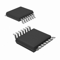
MRF49XA-I/ST Microchip Technology, MRF49XA-I/ST Datasheet - Page 58

MRF49XA-I/ST
Manufacturer Part Number
MRF49XA-I/ST
Description
IC RF TXRX 433/868/915 16-TSSOP
Manufacturer
Microchip Technology
Datasheet
1.MRF49XA-IST.pdf
(102 pages)
Specifications of MRF49XA-I/ST
Package / Case
16-TSSOP
Frequency
433MHz, 868MHz, 915MHz
Data Rate - Maximum
256kbps
Modulation Or Protocol
FHSS, FSK
Applications
Home / Industrial Automation, Remote Access, Security Alarms
Power - Output
7dbm
Sensitivity
-110dBm
Voltage - Supply
2.2 V ~ 3.8 V
Current - Receiving
11mA
Current - Transmitting
15mA
Data Interface
PCB, Surface Mount
Antenna Connector
PCB, Surface Mount
Operating Temperature
-40°C ~ 85°C
Number Of Receivers
1
Number Of Transmitters
2
Wireless Frequency
433 MHz to 915 MHz
Output Power
+ 7 dBm
Operating Supply Voltage
2.5 V, 3.3 V
Maximum Operating Temperature
+ 85 C
Mounting Style
SMD/SMT
Minimum Operating Temperature
- 40 C
Modulation
FHSS, FSK
Lead Free Status / RoHS Status
Lead free / RoHS Compliant
Memory Size
-
Lead Free Status / Rohs Status
Lead free / RoHS Compliant
Other names
579-MRF49XA-1/ST
Available stocks
Company
Part Number
Manufacturer
Quantity
Price
Company:
Part Number:
MRF49XA-I/ST
Manufacturer:
IR
Quantity:
450
Part Number:
MRF49XA-I/ST
Manufacturer:
MICROCHIP/微芯
Quantity:
20 000
DS70590B-page 56
MRF49XA
3.11
The Data Quality Indicator (DQI) is the digital process-
ing part of the radio connected to the demodulator and
functions when the receiver is on. This reports the
reception of an FSK modulated RF signal. The DQI
parameter setting defines how clean the incoming data
stream would be stated as good data (valid FSK
signal). The DIO signal goes high if the internally calcu-
lated data quality value exceeds the DIO threshold
parameter, for five consecutive data bits, for both high
and low periods.
The DQI parameter (i.e., Data Quality Threshold
Indicator (DQTI) bit) value is calculated using the
formula given in Equation 3-1.
EQUATION 3-1:
The DQI parameter in BBFCREG should be chosen
according to the following rules:
• The parameter should be > 4; otherwise, noise
• The maximum value is 7
Even during the on-time calculation in the Low Duty
Cycle mode, depending on the data quality threshold
indicator, the device needs to receive a few valid data
bits before the DQI signal indicates good signal condi-
tion (see Register 2-8). Selecting a short on-time can
FIGURE 3-10:
might be treated as a valid FSK signal
DQIpar = 4 x (Deviation – TX/RXoffset)/Bit Rate
Data Quality Indicator
CR_LOCK
CR_LOCK
DRSSI
DRSSI
DQI
DQI
DIO LOGIC BLOCK DIAGRAM
Preliminary
SET
CLR
FLIP/FLOP
DQI
R/S
prevent the crystal oscillator from starting, or the DQI
signal will not go high, even when the quality of the
received signal is good.
The DIO is an extension of the DQI. When incoming
data is detected, it uses the DQI signal, the clock recov-
ery lock signal and the digital RSSI signal to determine
if the incoming data is valid. The desired data rate and
the
user-programmable through the SPI port.
The DIO has three modes of operation: Slow, Medium
and Fast. Each mode is dependent on the signals it
uses to determine the valid data and also on the num-
ber of incoming preamble bits present at the beginning
of the packet.
The DIO can be disabled by the user so that only raw
data from the comparator comes out, or it can be set to
accept only a preset range of data rates and data
quality. The DIO saves the battery power and the time
for a host microcontroller because it will not wake-up
the microcontroller unless there is valid data present.
See Register 2-7 (RXCREG) for setup details.
The DIO signal is valid when using the internal receive
FIFO or an external pin to capture baseband data. DIO
can be multiplexed to pin 16 for external usage.
Figure 3-10 depicts the DIO logic block diagram.
Q
acceptance
LOGIC HIGH
MEDIUM
DIORT0
DIORT1
FAST
SLOW
RXCEN
© 2009 Microchip Technology Inc.
IN1
SEL0
SEL1
IN0
IN2
IN3
criteria
MUX
CLR
for
Y
valid
DIO
data
are


