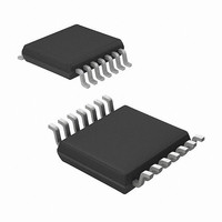
MRF49XA-I/ST Microchip Technology, MRF49XA-I/ST Datasheet - Page 21

MRF49XA-I/ST
Manufacturer Part Number
MRF49XA-I/ST
Description
IC RF TXRX 433/868/915 16-TSSOP
Manufacturer
Microchip Technology
Datasheet
1.MRF49XA-IST.pdf
(102 pages)
Specifications of MRF49XA-I/ST
Package / Case
16-TSSOP
Frequency
433MHz, 868MHz, 915MHz
Data Rate - Maximum
256kbps
Modulation Or Protocol
FHSS, FSK
Applications
Home / Industrial Automation, Remote Access, Security Alarms
Power - Output
7dbm
Sensitivity
-110dBm
Voltage - Supply
2.2 V ~ 3.8 V
Current - Receiving
11mA
Current - Transmitting
15mA
Data Interface
PCB, Surface Mount
Antenna Connector
PCB, Surface Mount
Operating Temperature
-40°C ~ 85°C
Number Of Receivers
1
Number Of Transmitters
2
Wireless Frequency
433 MHz to 915 MHz
Output Power
+ 7 dBm
Operating Supply Voltage
2.5 V, 3.3 V
Maximum Operating Temperature
+ 85 C
Mounting Style
SMD/SMT
Minimum Operating Temperature
- 40 C
Modulation
FHSS, FSK
Lead Free Status / RoHS Status
Lead free / RoHS Compliant
Memory Size
-
Lead Free Status / Rohs Status
Lead free / RoHS Compliant
Other names
579-MRF49XA-1/ST
Available stocks
Company
Part Number
Manufacturer
Quantity
Price
Company:
Part Number:
MRF49XA-I/ST
Manufacturer:
IR
Quantity:
450
Part Number:
MRF49XA-I/ST
Manufacturer:
MICROCHIP/微芯
Quantity:
20 000
REGISTER 2-1:
© 2009 Microchip Technology Inc.
bit 10
bit 9
bit 8
bit 7
bit 6
bit 5
bit 4
bit 3-0
Note 1:
Note:
2:
3:
4:
5:
All register commands begin with logic ‘1’ and only the STATUS register read command begins with logic ‘0’.
This bit is multiplexed for Transmit or Receive mode.
See the FFBC bits (FIFORSTREG<3:0>) in Register 2-10.
To get accurate values, the AFC should be disabled during the read by clearing the FOFEN bit
(AFCCREG<0>). The AFC offset value (OFFSB bits in the status word) is represented as a two’s
complement number. The actual frequency offset can be calculated as the AFC offset value multiplied by
the current PLL frequency step from CFSREG (FREQB<11:0>).
This bit is cleared after STSREG is read.
See Appendix A: “Read Sequence and Packet Structures” for the STSREG read sequence,.
LBTD: Low Battery Threshold Detect bit
Indicates whether the battery or supply voltage is below the preprogrammed threshold limit.
1 = Supply voltage is below threshold
0 = Normal supply voltage feed
FIFOEM: FIFO Empty bit
Indicates whether the receive FIFO is empty or filled.
1 = FIFO is empty
0 = FIFO is filled
ATRSSI: Antenna Tuning and Received Signal Strength Indicator bit
Transmit mode:
The bit indicates that the antenna tuning circuit has detected a strong RF signal.
1 = Strong RF signal present
0 = Weak or absence of RF signal
Receive mode:
The bit indicates that the incoming RF signal is above the preprogrammed digital RSSI limit.
1 = RF signal is above the threshold value set
0 = RF signal is less than the threshold value set
DQDO: Data Quality Detect/Indicate Output bit
Indicates good data quality output.
1 = Quality data is detected
0 = Quality data is unavailable
CLKRL: Clock Recovery Lock bit
Indicates clock recovery is locked.
1 = Clock recovery locked
0 = Clock recovery unlocked
AFCCT: Automatic Frequency Control Cycle Toggle bit
For each AFC cycle run, this bit toggles between logic ‘1’ and logic ‘0’.
1 = AFC cycle has occurred
0 = No AFC in this cycle
OFFSV: Offset Sign Value bit
Indicates the measured difference or frequency offset of any AFC cycle (sign of the offset value).
1 = Higher than the chip frequency
0 = Lower than the chip frequency
OFFSB<3:0>: Offset bits
The offset value to be added to the frequency control parameter (internal PLL).
1 = Result is negative
0 = Result is positive
STSREG: STATUS READ REGISTER (POR: 0x0000)
Preliminary
(1)
(CONTINUED)
MRF49XA
(4)
DS70590B-page 19


