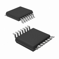
MRF49XA-I/ST Microchip Technology, MRF49XA-I/ST Datasheet - Page 29

MRF49XA-I/ST
Manufacturer Part Number
MRF49XA-I/ST
Description
IC RF TXRX 433/868/915 16-TSSOP
Manufacturer
Microchip Technology
Datasheet
1.MRF49XA-IST.pdf
(102 pages)
Specifications of MRF49XA-I/ST
Package / Case
16-TSSOP
Frequency
433MHz, 868MHz, 915MHz
Data Rate - Maximum
256kbps
Modulation Or Protocol
FHSS, FSK
Applications
Home / Industrial Automation, Remote Access, Security Alarms
Power - Output
7dbm
Sensitivity
-110dBm
Voltage - Supply
2.2 V ~ 3.8 V
Current - Receiving
11mA
Current - Transmitting
15mA
Data Interface
PCB, Surface Mount
Antenna Connector
PCB, Surface Mount
Operating Temperature
-40°C ~ 85°C
Number Of Receivers
1
Number Of Transmitters
2
Wireless Frequency
433 MHz to 915 MHz
Output Power
+ 7 dBm
Operating Supply Voltage
2.5 V, 3.3 V
Maximum Operating Temperature
+ 85 C
Mounting Style
SMD/SMT
Minimum Operating Temperature
- 40 C
Modulation
FHSS, FSK
Lead Free Status / RoHS Status
Lead free / RoHS Compliant
Memory Size
-
Lead Free Status / Rohs Status
Lead free / RoHS Compliant
Other names
579-MRF49XA-1/ST
Available stocks
Company
Part Number
Manufacturer
Quantity
Price
Company:
Part Number:
MRF49XA-I/ST
Manufacturer:
IR
Quantity:
450
Part Number:
MRF49XA-I/ST
Manufacturer:
MICROCHIP/微芯
Quantity:
20 000
REGISTER 2-7:
© 2009 Microchip Technology Inc.
bit 15
bit 7
Legend:
R = Readable bit
-n = Value at POR
bit 15-11
bit 10
bit 9-8
bit 7-5
bit 4-3
R/W-1
R/W-1
RXBW<2:0>
CCB<15:11>: Command Code bits
The command code bits (10010b) are serially sent to the microcontroller to identify the bits to be
written in the RXCREG.
FINTDIO: Function Interrupt/Data Indicator Output bit
Sets the pin 16 function as the data indicator output or interrupt.
1 = DIO output
0 = INT input
DIORT<1:0>: Data Indicator Output Response Time bits
If pin 16 is selected as DIO, these bits set the response time within which the transceiver detects and
indicates the incoming synchronous bit pattern, and issues an interrupt to the host microcontroller.
11 = Continuous
10 = Slow
01 = Medium
00 = Fast
RXBW<2:0>: Receiver Baseband Bandwidth bits
These bits set the bandwidth of demodulated data. The bandwidth can accommodate different data
rates and deviations during frequency keying.
111 = Reserved
110 = 67 kHz
101 = 134 kHz
100 = 200 kHz
011 = 270 kHz
010 = 340 kHz
001 = 400 kHz
000 = Reserved
RXLNA<1:0>: Receiver LNA Gain bits
These bits, when set to different values, can accommodate environments with high interferences. The
LNA gain also affects the true RSSI value.
11 = -20 dB
10 = -14 dB
01 = -6 dB
00 = 0 dB
R/W-0
R/W-0
RXCREG: RECEIVE CONTROL REGISTER (POR: 0x9080)
CCB<15:11>
r = reserved bit
W = Writable bit
‘1’ = Bit is set
R/W-0
R/W-0
R/W-1
R/W-0
Preliminary
RXLNA<1:0>
U = Unimplemented bit, read as ‘0’
‘0’ = Bit is cleared
R/W-0
R/W-0
FINTDIO
R/W-0
R/W-0
DRSSIT<2:0>
x = Bit is unknown
MRF49XA
R/W-0
R/W-0
DIORT<1:0>
DS70590B-page 27
R/W-0
R/W-0
bit 8
bit 0


