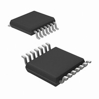
MRF49XA-I/ST Microchip Technology, MRF49XA-I/ST Datasheet - Page 9

MRF49XA-I/ST
Manufacturer Part Number
MRF49XA-I/ST
Description
IC RF TXRX 433/868/915 16-TSSOP
Manufacturer
Microchip Technology
Datasheet
1.MRF49XA-IST.pdf
(102 pages)
Specifications of MRF49XA-I/ST
Package / Case
16-TSSOP
Frequency
433MHz, 868MHz, 915MHz
Data Rate - Maximum
256kbps
Modulation Or Protocol
FHSS, FSK
Applications
Home / Industrial Automation, Remote Access, Security Alarms
Power - Output
7dbm
Sensitivity
-110dBm
Voltage - Supply
2.2 V ~ 3.8 V
Current - Receiving
11mA
Current - Transmitting
15mA
Data Interface
PCB, Surface Mount
Antenna Connector
PCB, Surface Mount
Operating Temperature
-40°C ~ 85°C
Number Of Receivers
1
Number Of Transmitters
2
Wireless Frequency
433 MHz to 915 MHz
Output Power
+ 7 dBm
Operating Supply Voltage
2.5 V, 3.3 V
Maximum Operating Temperature
+ 85 C
Mounting Style
SMD/SMT
Minimum Operating Temperature
- 40 C
Modulation
FHSS, FSK
Lead Free Status / RoHS Status
Lead free / RoHS Compliant
Memory Size
-
Lead Free Status / Rohs Status
Lead free / RoHS Compliant
Other names
579-MRF49XA-1/ST
Available stocks
Company
Part Number
Manufacturer
Quantity
Price
Company:
Part Number:
MRF49XA-I/ST
Manufacturer:
IR
Quantity:
450
Part Number:
MRF49XA-I/ST
Manufacturer:
MICROCHIP/微芯
Quantity:
20 000
2.0
The MRF49XA is an integrated, single chip ISM Band
Sub-GHz Transceiver. A simplified architectural block
diagram of the MRF49XA is shown in Figure 2-1.
The frequency synthesizer is clocked by an external
10 MHz crystal and generates the 433, 868 and
915 MHz radio frequency. The receiver with a Zero-IF
architecture consists of the following components:
• Low Noise Amplifier
• Down Conversion Mixers
• Channel Filters
• Baseband Limiting Amplifiers
• Receiver Signal Strength Indicator
The transmitter with a direct conversion architecture
has a typical output power of +7 dBm. An internal
transmit/receive switch combines the transmitter and
receiver circuits into differential RFP and RFN pins.
These pins are connected to the impedance matching
circuitry (Balun) and to the external antenna connected
to the device.
The device operates in the low-voltage range of 2.2V to
3.8V, and in Sleep mode, it operates at a very low-current
state, typically 0.3 μA.
© 2009 Microchip Technology Inc.
HARDWARE DESCRIPTION
Preliminary
The quality of the data is checked or validated using the
RSSI and DQI blocks built into the transceiver. Data is
buffered in transmitter registers and receiver FIFOs. The
Automatic Frequency Control feature allows the use of a
low-accuracy and low-cost crystal. The CLKOUT is used
to clock the external controller. The transceiver is con-
trolled via a 4-wire SPI, interrupt (INT/DIO and IRO),
FSK/DATA/FSEL, RCLKOUT/FCAP/FINT and RESET
pins. See Table 2-1 for pin details.
The MRF49XA supports the following feature blocks:
• Clock Generation
• Data Filtering and Amplification
• Data Pattern Recognition and Timing
• Data Processing and Storage
• Independent Transmit and Receiver FIFO Buffers
• Registers
These features reduce the processing load, and hence,
allows the use of low-cost 8-bit microcontrollers for
data processing.
MRF49XA
DS70590B-page 7


