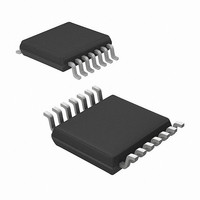
MRF49XA-I/ST Microchip Technology, MRF49XA-I/ST Datasheet - Page 47

MRF49XA-I/ST
Manufacturer Part Number
MRF49XA-I/ST
Description
IC RF TXRX 433/868/915 16-TSSOP
Manufacturer
Microchip Technology
Datasheet
1.MRF49XA-IST.pdf
(102 pages)
Specifications of MRF49XA-I/ST
Package / Case
16-TSSOP
Frequency
433MHz, 868MHz, 915MHz
Data Rate - Maximum
256kbps
Modulation Or Protocol
FHSS, FSK
Applications
Home / Industrial Automation, Remote Access, Security Alarms
Power - Output
7dbm
Sensitivity
-110dBm
Voltage - Supply
2.2 V ~ 3.8 V
Current - Receiving
11mA
Current - Transmitting
15mA
Data Interface
PCB, Surface Mount
Antenna Connector
PCB, Surface Mount
Operating Temperature
-40°C ~ 85°C
Number Of Receivers
1
Number Of Transmitters
2
Wireless Frequency
433 MHz to 915 MHz
Output Power
+ 7 dBm
Operating Supply Voltage
2.5 V, 3.3 V
Maximum Operating Temperature
+ 85 C
Mounting Style
SMD/SMT
Minimum Operating Temperature
- 40 C
Modulation
FHSS, FSK
Lead Free Status / RoHS Status
Lead free / RoHS Compliant
Memory Size
-
Lead Free Status / Rohs Status
Lead free / RoHS Compliant
Other names
579-MRF49XA-1/ST
Available stocks
Company
Part Number
Manufacturer
Quantity
Price
Company:
Part Number:
MRF49XA-I/ST
Manufacturer:
IR
Quantity:
450
Part Number:
MRF49XA-I/ST
Manufacturer:
MICROCHIP/微芯
Quantity:
20 000
FIGURE 3-3:
3.1.3
The Software Reset is initiated by using the host micro-
controller. The 0xFE00 command triggers this Reset
only if the Sensitive Reset mode is enabled. The hard-
ware automatically clears the bit(s) to their power-on
state. The Software Reset command is the same as
POR, but the duration of the Reset event is much less
than the actual POR (0.25 ms, typical).
3.1.4
The MRF49XA has an open-drain Reset output with an
internal pull-up and input buffer (active-low). The host
microcontroller resets the MRF49XA by asserting the
RESET pin to low (see Figure 3-4). All control registers
are reset to their POR values. The RESET pin consists
of an internal weak pull-up resistor. In order to allow the
RF circuitry to start-up and get stabilized, a delay of
around 0.25 ms is recommended for accessing the
MRF49XA after a hardware Reset.
FIGURE 3-4:
© 2009 Microchip Technology Inc.
To M CU Reset
(Input/Output*)
RESET
Pin
* These pins can be left floating.
(Pin 10)
RESET
Output
SOFTWARE RESET
RESET PIN
250 mV
V
V
DD
V
SS
H
L
DD
SENSITIVE RESET DISABLED
RESET PIN INTERNAL
CONNECTION
N
100k
Voltage (600 m V)
Reset Threshold
Reset Logic
To Internal
From POR
Circuit
10k
Preliminary
The registers associated with Reset are:
• STSREG (see Register 2-1)
• FIFORSTREG (see Register 2-10)
• WTSREG (see Register 2-14)
3.2
During the Reset event (caused by power-on, glitch on
the supply line or Software Reset), the V
be kept clean. Noise or a periodic disturbing signal
superimposed on the supply voltage may prevent the
device from getting out of the Reset state. To avoid this,
adequate filters should be made available on the power
supply lines to keep the distorting signal level below
100 mVp-p, in the DC-50 kHz range for 200 ms, from
V
sometimes introduce switching noise on the V
so follow the power supply manufacturer’s recommen-
dations on how to decrease the ripple of regulator IC
and/or how to shift the switching frequency while using
SMPS.
The registers associated with power line filtering are:
• STSREG (see Register 2-1)
• FIFORSTREG (see Register 2-10)
• WTSREG (see Register 2-14)
DD
ramp start. The usage of regulators or SMPS may
V
DD
Line Filtering
Reset Ramp Line
MRF49XA
(100 mV/ms)
DS70590B-page 45
Tim e
DD
line should
DD
line,


