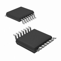
MRF49XA-I/ST Microchip Technology, MRF49XA-I/ST Datasheet - Page 59

MRF49XA-I/ST
Manufacturer Part Number
MRF49XA-I/ST
Description
IC RF TXRX 433/868/915 16-TSSOP
Manufacturer
Microchip Technology
Datasheet
1.MRF49XA-IST.pdf
(102 pages)
Specifications of MRF49XA-I/ST
Package / Case
16-TSSOP
Frequency
433MHz, 868MHz, 915MHz
Data Rate - Maximum
256kbps
Modulation Or Protocol
FHSS, FSK
Applications
Home / Industrial Automation, Remote Access, Security Alarms
Power - Output
7dbm
Sensitivity
-110dBm
Voltage - Supply
2.2 V ~ 3.8 V
Current - Receiving
11mA
Current - Transmitting
15mA
Data Interface
PCB, Surface Mount
Antenna Connector
PCB, Surface Mount
Operating Temperature
-40°C ~ 85°C
Number Of Receivers
1
Number Of Transmitters
2
Wireless Frequency
433 MHz to 915 MHz
Output Power
+ 7 dBm
Operating Supply Voltage
2.5 V, 3.3 V
Maximum Operating Temperature
+ 85 C
Mounting Style
SMD/SMT
Minimum Operating Temperature
- 40 C
Modulation
FHSS, FSK
Lead Free Status / RoHS Status
Lead free / RoHS Compliant
Memory Size
-
Lead Free Status / Rohs Status
Lead free / RoHS Compliant
Other names
579-MRF49XA-1/ST
Available stocks
Company
Part Number
Manufacturer
Quantity
Price
Company:
Part Number:
MRF49XA-I/ST
Manufacturer:
IR
Quantity:
450
Part Number:
MRF49XA-I/ST
Manufacturer:
MICROCHIP/微芯
Quantity:
20 000
The DIO signal response time setting is configured
through RXCREG and has the following modes of
operation:
• Default mode: The DIO is permanently
• Slow mode: The DIO signal goes high if the
• Medium mode: The DIO signal is active when the
• Fast mode: The DIO signal follows the level of
The registers associated with DQI are:
• STSREG (see Register 2-1)
• RXCREG (see Register 2-7)
• BBFCREG (see Register 2-8)
3.12
The internal synchronous pattern and the pattern
length are user-programmable. The MRF49XA is con-
figured to use a synchronous character to indicate the
valid incoming data. The synchronous character selec-
tion is done through the FIFORSTREG. The character
is divided into two bytes: SCL1 and SCL0. The SCL0
byte is user-configurable, whereas SCL1 is fixed to
2Dh and is non-programmable. The synchronous char-
acter can also be configured as a byte character or a
word character. A byte character uses only SCL0,
whereas the word character uses both SCL1 and
SCL0. Since SCL0 is user-configurable, it is advanta-
geous while operating under interferences and also
while identifying the related transmitters.
The registers associated with the programmable
synchronous byte are:
• FIFORSTREG (see Register 2-10)
• PMCREG (see Register 2-13)
© 2009 Microchip Technology Inc.
connected to logic high. It always stays high
independent of the receiving parameters.
digital RSSI, DQI and Clock Recovery Lock
(CR_LOCK) signals are present. It stays high until
any of these signals are present and goes low
when all three input signals are low.
CR_LOCK and the DRSSI or the DQI signals are
high. It goes low when either the CR_LOCK
becomes inactive or the DRSSI or DQI signals
goes low.
the DQI signal.
Programmable Synchronous Byte
Preliminary
3.13
The Received Signal Strength Indicator (RSSI) estimates
the received signal power within the bandwidth of ISM
channels. The MRF49XA provides both analog RSSI
and digital RSSI. A digital RSSI output is provided to
monitor the input signal level. The signal goes high if the
received signal strength exceeds a given pre-
programmed level. The digital RSSI threshold is
programmable through RXCREG, and is read and moni-
tored only through STSREG. When an incoming signal is
stronger than the preprogrammed threshold, the digital
RSSI bit in the STSREG is set. The settling time of digital
RSSI depends on the external filter capacitor.
The DRSSIT value is a 3-bit binary value ranging from
0-8. Table 3-2 shows the mapping between the
DRSSIT value versus the received power level. The
number of symbols to average can be changed by
programming the DRSSIT bits (RXCREG<2:0>).
The digital RSSI is basically a sensitive comparator
behind an analog RSSI block. The comparator thresh-
old can be set using the three bits and the comparator
output can be read out through the Status Read
register. The curve in Figure 3-11 shows the analog
RSSI output voltage versus signal strength.
The analog RSSI level is linear with input signal levels
between -103 and -73 dBm. The RSSIO pin in
MRF49XA is used as an analog RSSI output and better
results can be achieved by using this pin with a
sensitive comparator.
These bits can be set to indicate the incoming signal
strength above a preset limit. The result enables or
disables the DQDO bit (STSREG<7>). The RSSI
threshold depends on the LNA gain and the real RSSI
threshold can be calculated by using the formula as
given in Equation 3-2.
EQUATION 3-2:
In Transmit mode, the ATRSSI bit (STSREG<8>)
indicates that the antenna tuning circuit has detected a
relatively strong RF signal.
In Receive mode, the ATRSSI bit indicates that the
incoming RF signal is above the preprogrammed digital
RSSI threshold.
Received Signal Strength
Indicator
RSSIth = RSSIsetth + GLNA
MRF49XA
DS70590B-page 57


