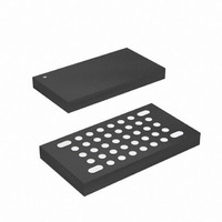
ATMEGA16HVA-4CKU Atmel, ATMEGA16HVA-4CKU Datasheet - Page 108

ATMEGA16HVA-4CKU
Manufacturer Part Number
ATMEGA16HVA-4CKU
Description
MCU AVR 16K FLASH 4MHZ 36-LGA
Manufacturer
Atmel
Series
AVR® ATmegar
Datasheet
1.ATMEGA16HVA-4CKU.pdf
(196 pages)
Specifications of ATMEGA16HVA-4CKU
Core Processor
AVR
Core Size
8-Bit
Speed
4MHz
Connectivity
SPI
Peripherals
Brown-out Detect/Reset, POR, PWM, WDT
Number Of I /o
7
Program Memory Size
16KB (8K x 16)
Program Memory Type
FLASH
Eeprom Size
256 x 8
Ram Size
512 x 8
Voltage - Supply (vcc/vdd)
1.8 V ~ 9 V
Data Converters
A/D 5x12b
Oscillator Type
External
Operating Temperature
-20°C ~ 85°C
Package / Case
36-LGA
Processor Series
ATMEGA16x
Core
AVR8
Data Bus Width
8 bit
Data Ram Size
512 B
Interface Type
SPI
Maximum Clock Frequency
4 MHz
Number Of Programmable I/os
6
Number Of Timers
2
Maximum Operating Temperature
+ 85 C
Mounting Style
SMD/SMT
3rd Party Development Tools
EWAVR, EWAVR-BL
Development Tools By Supplier
ATAVRDRAGON, ATSTK500, ATSTK600, ATAVRISP2, ATAVRONEKIT, ATAVRSB200, ATAVRSB201
Minimum Operating Temperature
- 20 C
On-chip Adc
12 bit, 5 Channel
For Use With
ATSTK600 - DEV KIT FOR AVR/AVR32ATSTK500 - PROGRAMMER AVR STARTER KIT
Lead Free Status / RoHS Status
Lead free / RoHS Compliant
- Current page: 108 of 196
- Download datasheet (3Mb)
108
ATmega8HVA/16HVA
• Bit 5 - CADUB: CC-ADC Update Busy
The CC-ADC operates in a different clock domain than the CPU. Whenever a new value is writ-
ten to CADCSRA or CADRC this value must be synchronized to the CCADC clock domain.
Subsequent writes to these registers will be blocked during this synchronization. Synchroniza-
tion of one of the registers will block updating of all the others. The CADUB bit will be read as
one while any of these registers is being synchronized, and will be read as zero when neither
register is being synchronized.
• Bits 4:3: CADAS[1:0]: CC-ADC Accumulate Current Select
The CADAS bits select the conversion time for the Accumulate Current output as shown in
19-1.
Table 19-1.
Note:
”Slow RC Oscillator” on page 26
• Bits 2:1: CADSI[1:0]: CC-ADC Current Sampling Interval
The CADSI bits determine the current sampling interval for the Regular Current detection as
shown in
Table 19-2.
Notes:
• Bit 0 - CADSE: CC-ADC Sampling Enable
When the CADSE bit is written to one, the ongoing CC-ADC conversion is aborted, and the
CCADC enters Regular Current detection mode.
1. The actual value depends on the actual frequency of the Slow RC oscillator, see
1. The actual value depends on the actual frequency of the Slow RC oscillator, see
2. Sampling time ~ 12 ms.
Table
CADAS[1:0]
CADSI[1:0]
Oscillator” on page 26
CC-ADC Accumulate Current Conversion Time
CC-ADC Regular Current Sampling Interval
00
01
10
11
00
01
10
11
19-2.
.
.
CC-ADC Accumulate Current
CC-ADC Regular Current
250 ms (+ sampling time)
500 ms (+ sampling time)
Sampling Interval
1s (+ sampling time)
2s (+ sampling time)
Conversion Time
125 ms
250 ms
500 ms
1s
(1)(2)
(1)
Number of CC-ADC Clock
Number of CC-ADC Clock
16384 (+ sampling time)
32768 (+ sampling time)
65536 (+ sampling time)
8192 (+ sampling time)
Cycles
Cycles
16384
32768
4096
8192
8024A–AVR–04/08
”Slow RC
Table
Related parts for ATMEGA16HVA-4CKU
Image
Part Number
Description
Manufacturer
Datasheet
Request
R

Part Number:
Description:
DEV KIT FOR AVR/AVR32
Manufacturer:
Atmel
Datasheet:

Part Number:
Description:
INTERVAL AND WIPE/WASH WIPER CONTROL IC WITH DELAY
Manufacturer:
ATMEL Corporation
Datasheet:

Part Number:
Description:
Low-Voltage Voice-Switched IC for Hands-Free Operation
Manufacturer:
ATMEL Corporation
Datasheet:

Part Number:
Description:
MONOLITHIC INTEGRATED FEATUREPHONE CIRCUIT
Manufacturer:
ATMEL Corporation
Datasheet:

Part Number:
Description:
AM-FM Receiver IC U4255BM-M
Manufacturer:
ATMEL Corporation
Datasheet:

Part Number:
Description:
Monolithic Integrated Feature Phone Circuit
Manufacturer:
ATMEL Corporation
Datasheet:

Part Number:
Description:
Multistandard Video-IF and Quasi Parallel Sound Processing
Manufacturer:
ATMEL Corporation
Datasheet:

Part Number:
Description:
High-performance EE PLD
Manufacturer:
ATMEL Corporation
Datasheet:

Part Number:
Description:
8-bit Flash Microcontroller
Manufacturer:
ATMEL Corporation
Datasheet:

Part Number:
Description:
2-Wire Serial EEPROM
Manufacturer:
ATMEL Corporation
Datasheet:


