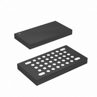
ATMEGA16HVA-4CKU Atmel, ATMEGA16HVA-4CKU Datasheet - Page 153

ATMEGA16HVA-4CKU
Manufacturer Part Number
ATMEGA16HVA-4CKU
Description
MCU AVR 16K FLASH 4MHZ 36-LGA
Manufacturer
Atmel
Series
AVR® ATmegar
Datasheet
1.ATMEGA16HVA-4CKU.pdf
(196 pages)
Specifications of ATMEGA16HVA-4CKU
Core Processor
AVR
Core Size
8-Bit
Speed
4MHz
Connectivity
SPI
Peripherals
Brown-out Detect/Reset, POR, PWM, WDT
Number Of I /o
7
Program Memory Size
16KB (8K x 16)
Program Memory Type
FLASH
Eeprom Size
256 x 8
Ram Size
512 x 8
Voltage - Supply (vcc/vdd)
1.8 V ~ 9 V
Data Converters
A/D 5x12b
Oscillator Type
External
Operating Temperature
-20°C ~ 85°C
Package / Case
36-LGA
Processor Series
ATMEGA16x
Core
AVR8
Data Bus Width
8 bit
Data Ram Size
512 B
Interface Type
SPI
Maximum Clock Frequency
4 MHz
Number Of Programmable I/os
6
Number Of Timers
2
Maximum Operating Temperature
+ 85 C
Mounting Style
SMD/SMT
3rd Party Development Tools
EWAVR, EWAVR-BL
Development Tools By Supplier
ATAVRDRAGON, ATSTK500, ATSTK600, ATAVRISP2, ATAVRONEKIT, ATAVRSB200, ATAVRSB201
Minimum Operating Temperature
- 20 C
On-chip Adc
12 bit, 5 Channel
For Use With
ATSTK600 - DEV KIT FOR AVR/AVR32ATSTK500 - PROGRAMMER AVR STARTER KIT
Lead Free Status / RoHS Status
Lead free / RoHS Compliant
- Current page: 153 of 196
- Download datasheet (3Mb)
8024A–AVR–04/08
3. The serial programming instructions will not work if the communication is out of synchro-
4. The Flash is programmed one page at a time. The memory page is loaded one byte at a
5. A: The EEPROM array is programmed one byte at a time by supplying the address and
6. Any memory location can be verified by using the Read instruction which returns the con-
7. At the end of the programming session, RESET can be set high to commence normal
8. Power-off sequence (if needed):
Table 27-9.
Symbol
t
t
t
t
WD_FLASH
WD_EEPROM
WD_ERASE
WD_FUSE
nization. When in sync. the second byte (0x53), will echo back when issuing the third
byte of the Programming Enable instruction. Whether the echo is correct or not, all four
bytes of the instruction must be transmitted. If the 0x53 did not echo back, give RESET a
positive pulse and issue a new Programming Enable command.
time by supplying the 5 LSB of the address and data together with the Load Program
memory Page instruction. To ensure correct loading of the page, the data low byte must
be loaded before data high byte is applied for a given address. The Program memory
Page is stored by loading the Write Program memory Page instruction with the 6 MSB of
the address. If polling (RDY/BSY) is not used, the user must wait at least t
issuing the next page. (See
before the Flash write operation completes can result in incorrect programming.
data together with the appropriate Write instruction. An EEPROM memory location is first
automatically erased before new data is written. If polling (RDY/BSY) is not used, the
user must wait at least t
chip erased device, no 0xFFs in the data file(s) need to be programmed.
B: The EEPROM array is programmed one page at a time. The Memory page is loaded
one byte at a time by supplying the 2 LSB of the address and data together with the Load
EEPROM Memory Page instruction. The EEPROM Memory Page is stored by loading
the Write EEPROM Memory Page Instruction with the 6 MSB of the address. When using
EEPROM page access only byte locations loaded with the Load EEPROM Memory Page
instruction is altered. The remaining locations remain unchanged. If polling (RDY/BSY) is
not used, the used must wait at least t
27-7 on page
programmed.
tent at the selected address at serial output MISO.
operation.
Set RESET to “1”.
Turn V
CC
power off.
Minimum Wait Delay Before Writing the Next Flash or EEPROM Location
151). In a chip erased device, no 0xFF in the data file(s) need to be
WD_EEPROM
Table
27-9.) Accessing the serial programming interface
before issuing the next byte. (See
WD_EEPROM
before issuing the next page (See
ATmega8HVA/16HVA
Minimum Wait Delay
4.5 ms
4.0 ms
4.0 ms
4.5 ms
Table
WD_FLASH
27-9.) In a
before
Table
153
Related parts for ATMEGA16HVA-4CKU
Image
Part Number
Description
Manufacturer
Datasheet
Request
R

Part Number:
Description:
DEV KIT FOR AVR/AVR32
Manufacturer:
Atmel
Datasheet:

Part Number:
Description:
INTERVAL AND WIPE/WASH WIPER CONTROL IC WITH DELAY
Manufacturer:
ATMEL Corporation
Datasheet:

Part Number:
Description:
Low-Voltage Voice-Switched IC for Hands-Free Operation
Manufacturer:
ATMEL Corporation
Datasheet:

Part Number:
Description:
MONOLITHIC INTEGRATED FEATUREPHONE CIRCUIT
Manufacturer:
ATMEL Corporation
Datasheet:

Part Number:
Description:
AM-FM Receiver IC U4255BM-M
Manufacturer:
ATMEL Corporation
Datasheet:

Part Number:
Description:
Monolithic Integrated Feature Phone Circuit
Manufacturer:
ATMEL Corporation
Datasheet:

Part Number:
Description:
Multistandard Video-IF and Quasi Parallel Sound Processing
Manufacturer:
ATMEL Corporation
Datasheet:

Part Number:
Description:
High-performance EE PLD
Manufacturer:
ATMEL Corporation
Datasheet:

Part Number:
Description:
8-bit Flash Microcontroller
Manufacturer:
ATMEL Corporation
Datasheet:

Part Number:
Description:
2-Wire Serial EEPROM
Manufacturer:
ATMEL Corporation
Datasheet:


