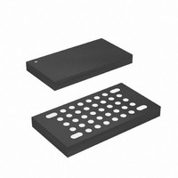
ATMEGA16HVA-4CKU Atmel, ATMEGA16HVA-4CKU Datasheet - Page 143

ATMEGA16HVA-4CKU
Manufacturer Part Number
ATMEGA16HVA-4CKU
Description
MCU AVR 16K FLASH 4MHZ 36-LGA
Manufacturer
Atmel
Series
AVR® ATmegar
Datasheet
1.ATMEGA16HVA-4CKU.pdf
(196 pages)
Specifications of ATMEGA16HVA-4CKU
Core Processor
AVR
Core Size
8-Bit
Speed
4MHz
Connectivity
SPI
Peripherals
Brown-out Detect/Reset, POR, PWM, WDT
Number Of I /o
7
Program Memory Size
16KB (8K x 16)
Program Memory Type
FLASH
Eeprom Size
256 x 8
Ram Size
512 x 8
Voltage - Supply (vcc/vdd)
1.8 V ~ 9 V
Data Converters
A/D 5x12b
Oscillator Type
External
Operating Temperature
-20°C ~ 85°C
Package / Case
36-LGA
Processor Series
ATMEGA16x
Core
AVR8
Data Bus Width
8 bit
Data Ram Size
512 B
Interface Type
SPI
Maximum Clock Frequency
4 MHz
Number Of Programmable I/os
6
Number Of Timers
2
Maximum Operating Temperature
+ 85 C
Mounting Style
SMD/SMT
3rd Party Development Tools
EWAVR, EWAVR-BL
Development Tools By Supplier
ATAVRDRAGON, ATSTK500, ATSTK600, ATAVRISP2, ATAVRONEKIT, ATAVRSB200, ATAVRSB201
Minimum Operating Temperature
- 20 C
On-chip Adc
12 bit, 5 Channel
For Use With
ATSTK600 - DEV KIT FOR AVR/AVR32ATSTK500 - PROGRAMMER AVR STARTER KIT
Lead Free Status / RoHS Status
Lead free / RoHS Compliant
- Current page: 143 of 196
- Download datasheet (3Mb)
26.2.1
26.2.2
26.2.3
26.2.4
8024A–AVR–04/08
EEPROM Write Prevents Writing to SPMCSR
Setting the Lock Bits from Software
Reading the Fuse and Lock Bits from Software
Preventing Flash Corruption
Note that an EEPROM write operation will block all software programming to Flash. Reading the
Fuses and Lock bits from software will also be prevented during the EEPROM write operation. It
is recommended that the user checks the status bit (EEPE) in the EECR Register and verifies
that the bit is cleared before writing to the SPMCSR Register.
To set the Lock Bits, write the desired data to R0. If bits 1..0 in R0 are cleared (zero), the corre-
sponding Lock bit will be programmed if an SPM instruction is executed within four cycles after
RFLB and SPMEN are set in SPMCSR. The Z-pointer is don’t care during this operation, but for
future compatibility it is recommended to load the Z-pointer with 0x0001 (same as used for read-
ing the Lock bits). For future compatibility it is also recommended to set bit 7..2 in R0 to “1” when
writing the Lock bits. When programming the Lock bits the entire Flash can be read during the
operation.
See
Lock bits affect the Flash access.
It is possible to read both the Fuse and Lock bits from software. To read the Lock bits, load the
Z-pointer with 0x0001 and set the RFLB and SPMEN bits in SPMCSR. When an LPM instruction
is executed within three CPU cycles after the RFLB and SPMEN bits are set in SPMCSR, the
value of the Lock bits will be loaded in the destination register. The RFLB and SPMEN bits will
auto-clear 6 cycles after writing to SPMCSR if no SPM instruction is executed within four CPU
cycles. SPMCSR is locked for further writing until it is auto-cleared. The LPM instruction must be
executed within three CPU cycles after writing SPMCSR. When RFLB and SPMEN are cleared,
LPM will work as described in the Instruction set Manual.
The algorithm for reading the Fuse Low byte is similar to the one described above for reading
the Lock bits. To read the Fuse Low byte, load the Z-pointer with 0x0000 and set the RFLB and
SPMEN bits in SPMCSR. When an LPM instruction is executed within three cycles after the
RFLB and SPMEN bits are set in the SPMCSR, the value of the Fuse Low byte (FLB) will be
loaded in the destination register as shown below. Refer to
detailed description and mapping of the Fuse Low byte.
Fuse and Lock bits that are programmed, will be read as zero. Fuse and Lock bits that are
unprogrammed, will be read as one.
During periods of low V
too low for the CPU and the Flash to operate properly. These issues are the same as for board
level systems using the Flash, and the same design solutions should be applied.
Bit
R0
Bit
Rd
Bit
Rd
Table 27-1 on page 149
FLB7
7
1
7
7
–
CC
FLB6
, the Flash program can be corrupted because the supply voltage is
6
1
6
6
–
and
FLB5
Table 27-2 on page 149
5
1
5
5
–
FLB4
4
1
4
–
4
FLB3
3
1
3
–
3
ATmega8HVA/16HVA
for how the different settings of the
FLB2
2
1
2
–
2
Table 27-4 on page 150
FLB1
LB2
LB2
1
1
1
FLB0
LB1
LB1
0
0
0
for a
143
Related parts for ATMEGA16HVA-4CKU
Image
Part Number
Description
Manufacturer
Datasheet
Request
R

Part Number:
Description:
DEV KIT FOR AVR/AVR32
Manufacturer:
Atmel
Datasheet:

Part Number:
Description:
INTERVAL AND WIPE/WASH WIPER CONTROL IC WITH DELAY
Manufacturer:
ATMEL Corporation
Datasheet:

Part Number:
Description:
Low-Voltage Voice-Switched IC for Hands-Free Operation
Manufacturer:
ATMEL Corporation
Datasheet:

Part Number:
Description:
MONOLITHIC INTEGRATED FEATUREPHONE CIRCUIT
Manufacturer:
ATMEL Corporation
Datasheet:

Part Number:
Description:
AM-FM Receiver IC U4255BM-M
Manufacturer:
ATMEL Corporation
Datasheet:

Part Number:
Description:
Monolithic Integrated Feature Phone Circuit
Manufacturer:
ATMEL Corporation
Datasheet:

Part Number:
Description:
Multistandard Video-IF and Quasi Parallel Sound Processing
Manufacturer:
ATMEL Corporation
Datasheet:

Part Number:
Description:
High-performance EE PLD
Manufacturer:
ATMEL Corporation
Datasheet:

Part Number:
Description:
8-bit Flash Microcontroller
Manufacturer:
ATMEL Corporation
Datasheet:

Part Number:
Description:
2-Wire Serial EEPROM
Manufacturer:
ATMEL Corporation
Datasheet:


