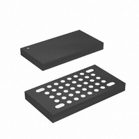
ATMEGA16HVA-4CKU Atmel, ATMEGA16HVA-4CKU Datasheet - Page 113

ATMEGA16HVA-4CKU
Manufacturer Part Number
ATMEGA16HVA-4CKU
Description
MCU AVR 16K FLASH 4MHZ 36-LGA
Manufacturer
Atmel
Series
AVR® ATmegar
Datasheet
1.ATMEGA16HVA-4CKU.pdf
(196 pages)
Specifications of ATMEGA16HVA-4CKU
Core Processor
AVR
Core Size
8-Bit
Speed
4MHz
Connectivity
SPI
Peripherals
Brown-out Detect/Reset, POR, PWM, WDT
Number Of I /o
7
Program Memory Size
16KB (8K x 16)
Program Memory Type
FLASH
Eeprom Size
256 x 8
Ram Size
512 x 8
Voltage - Supply (vcc/vdd)
1.8 V ~ 9 V
Data Converters
A/D 5x12b
Oscillator Type
External
Operating Temperature
-20°C ~ 85°C
Package / Case
36-LGA
Processor Series
ATMEGA16x
Core
AVR8
Data Bus Width
8 bit
Data Ram Size
512 B
Interface Type
SPI
Maximum Clock Frequency
4 MHz
Number Of Programmable I/os
6
Number Of Timers
2
Maximum Operating Temperature
+ 85 C
Mounting Style
SMD/SMT
3rd Party Development Tools
EWAVR, EWAVR-BL
Development Tools By Supplier
ATAVRDRAGON, ATSTK500, ATSTK600, ATAVRISP2, ATAVRONEKIT, ATAVRSB200, ATAVRSB201
Minimum Operating Temperature
- 20 C
On-chip Adc
12 bit, 5 Channel
For Use With
ATSTK600 - DEV KIT FOR AVR/AVR32ATSTK500 - PROGRAMMER AVR STARTER KIT
Lead Free Status / RoHS Status
Lead free / RoHS Compliant
- Current page: 113 of 196
- Download datasheet (3Mb)
20.3.1
8024A–AVR–04/08
Configuring PA1 and PA0 for V-ADC operation
Power-off mode. Note that the bandgap voltage reference must be enabled and disabled sepa-
rately, see
Figure 20-2. Voltage ADC Conversion Diagram
To perform a V-ADC conversion, the analog input channel must first be selected by writing to the
VADMUX register. When a logical one is written to the V-ADC Start Conversion bit VADSC, a
conversion of the selected channel will start. The VADSC bit stays high as long as the conver-
sion is in progress and will be cleared by hardware when the conversion is completed. When a
conversion is in progress, the V-ADC Data Register - VADCL and VADCH will be invalid. If the
System Clock Prescaler setting is changed during a V-ADC conversion, the conversion will be
aborted. If a different data channel is selected while a conversion is in progress, the ADC will fin-
ish the current conversion before performing the channel change. When a conversion is finished
the V-ADC Conversion Complete Interrupt Flag – VADCCIF is set. One 12-bit conversion takes
519 µs to complete from the start bit is set to the interrupt flag is set. The V-ADC Data Register -
VADCL and VADCH will be valid until a new conversion is started. To ensure that correct data is
read, both high and low byte data registers should be read before starting a new conversion.
When one of the single ended channels ADC0 or ADC1 is used as analog input to the VADC,
either PA0 or PA1 are used as signal ground (SGND). When ADC0/1 is selected as input chan-
nel, PA1/0 is automatically switched to SGND.
The use of PA1 and PA0 as SGND is efficient for the thermistor configuration shown in
ing Circuit” on page
divider resistor, R1, to PA0 and PA1 respectively.
Both PA0 and PA1 have very high input impedance when used as ADC inputs, which makes it
possible to connect two thermistors in the configuration, shown in
162. However, input impedance is limited and if high accuracy is required, only one thermistor
should be connected between PA0 and PA1. If two termistors are connected, the configuration
is as follows:
• When measuring RT1, PA1 should be used as input channel and PA0 is automatically switched
• When measuring RT2, PA0 should be used as input channel and PA1 is automatically switched
Conversion Result
to SGND.
to SGND.
Start Conversion
Interrupt
”BGCCR – Bandgap Calibration C Register” on page
OLD DATA
162. Both termistors, RT1 and RT2, are connected through a common
INVALID DATA
V A L I D
ATmega8HVA/16HVA
D ATA
118.
”Operating Circuit” on page
INVALID DATA
”Operat-
113
Related parts for ATMEGA16HVA-4CKU
Image
Part Number
Description
Manufacturer
Datasheet
Request
R

Part Number:
Description:
DEV KIT FOR AVR/AVR32
Manufacturer:
Atmel
Datasheet:

Part Number:
Description:
INTERVAL AND WIPE/WASH WIPER CONTROL IC WITH DELAY
Manufacturer:
ATMEL Corporation
Datasheet:

Part Number:
Description:
Low-Voltage Voice-Switched IC for Hands-Free Operation
Manufacturer:
ATMEL Corporation
Datasheet:

Part Number:
Description:
MONOLITHIC INTEGRATED FEATUREPHONE CIRCUIT
Manufacturer:
ATMEL Corporation
Datasheet:

Part Number:
Description:
AM-FM Receiver IC U4255BM-M
Manufacturer:
ATMEL Corporation
Datasheet:

Part Number:
Description:
Monolithic Integrated Feature Phone Circuit
Manufacturer:
ATMEL Corporation
Datasheet:

Part Number:
Description:
Multistandard Video-IF and Quasi Parallel Sound Processing
Manufacturer:
ATMEL Corporation
Datasheet:

Part Number:
Description:
High-performance EE PLD
Manufacturer:
ATMEL Corporation
Datasheet:

Part Number:
Description:
8-bit Flash Microcontroller
Manufacturer:
ATMEL Corporation
Datasheet:

Part Number:
Description:
2-Wire Serial EEPROM
Manufacturer:
ATMEL Corporation
Datasheet:


