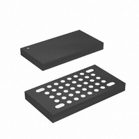
ATMEGA16HVA-4CKU Atmel, ATMEGA16HVA-4CKU Datasheet - Page 83

ATMEGA16HVA-4CKU
Manufacturer Part Number
ATMEGA16HVA-4CKU
Description
MCU AVR 16K FLASH 4MHZ 36-LGA
Manufacturer
Atmel
Series
AVR® ATmegar
Datasheet
1.ATMEGA16HVA-4CKU.pdf
(196 pages)
Specifications of ATMEGA16HVA-4CKU
Core Processor
AVR
Core Size
8-Bit
Speed
4MHz
Connectivity
SPI
Peripherals
Brown-out Detect/Reset, POR, PWM, WDT
Number Of I /o
7
Program Memory Size
16KB (8K x 16)
Program Memory Type
FLASH
Eeprom Size
256 x 8
Ram Size
512 x 8
Voltage - Supply (vcc/vdd)
1.8 V ~ 9 V
Data Converters
A/D 5x12b
Oscillator Type
External
Operating Temperature
-20°C ~ 85°C
Package / Case
36-LGA
Processor Series
ATMEGA16x
Core
AVR8
Data Bus Width
8 bit
Data Ram Size
512 B
Interface Type
SPI
Maximum Clock Frequency
4 MHz
Number Of Programmable I/os
6
Number Of Timers
2
Maximum Operating Temperature
+ 85 C
Mounting Style
SMD/SMT
3rd Party Development Tools
EWAVR, EWAVR-BL
Development Tools By Supplier
ATAVRDRAGON, ATSTK500, ATSTK600, ATAVRISP2, ATAVRONEKIT, ATAVRSB200, ATAVRSB201
Minimum Operating Temperature
- 20 C
On-chip Adc
12 bit, 5 Channel
For Use With
ATSTK600 - DEV KIT FOR AVR/AVR32ATSTK500 - PROGRAMMER AVR STARTER KIT
Lead Free Status / RoHS Status
Lead free / RoHS Compliant
17.6.1
17.6.2
17.6.3
8024A–AVR–04/08
Input Capture Trigger Source
Noise Canceler
Using the Input Capture Unit
When a change of the logic level (an event) occurs on the Input Capture pin (ICPx), and this
change confirms to the setting of the edge detector, a capture will be triggered. When a capture
is triggered, the value of the counter (TCNTn) is written to the Input Capture Register (ICRn).
The Input Capture Flag (ICFn) is set at the same system clock as the TCNTn value is copied into
Input Capture Register. If enabled (TICIEn=1), the Input Capture Flag generates an Input Cap-
ture interrupt. The ICFn flag is automatically cleared when the interrupt is executed. Alternatively
the ICFn flag can be cleared by software by writing a logical one to its I/O bit location.
The default trigger source for the Input Capture unit is the I/O port PC0 in Timer/Counter0 and
the Battery Protection Interrupt in Timer/Counter1. Alternatively can the osi_posedge pin on the
Oscillator Sampling Interface in Timer/Counter0 and Voltage Regulator Interrupt in
Timer/Counter1 be used as trigger sources. The osi_posedge pin in Timer/Counter0 Control
Register A (TCCR0A) and the Voltage Regulator Interrupt bit in the Timer/Counter1 Control
Register A (TCCR1A) is selected as trigger sources by setting the Input Capture Select bits
respectively to 00 and 11. Be aware that changing trigger source can trigger a capture. The
Input Capture Flag must therefore be cleared after the change.
Both Input Capture inputs are sampled using the same technique. The edge detector is also
identical. However, when the noise canceler is enabled, additional logic is inserted before the
edge detector, which increases the delay by four system clock cycles. An Input Capture on
Timer/Counter0 can also be triggered by software by controlling the port of the PC0 pin.
The noise canceler improves noise immunity by using a simple digital filtering scheme. The
noise canceler input is monitored over four samples, and all four must be equal for changing the
output that in turn is used by the edge detector.
The noise canceler is enabled by setting the Input Capture Noise Canceler (ICNCn) bit in
Timer/Counter Control Register n B (TCCRnB). When enabled the noise canceler introduces
additional four system clock cycles of delay from a change applied to the input, to the update of
the ICRn Register. The noise canceler uses the system clock and is therefore not affected by the
prescaler.
The main challenge when using the Input Capture unit is to assign enough processor capacity
for handling the incoming events. The time between two events is critical. If the processor has
not read the captured value in the ICRn Register before the next event occurs, the ICRn will be
overwritten with a new value. In this case the result of the capture will be incorrect.
When using the Input Capture interrupt, the ICRn Register should be read as early in the inter-
rupt handler routine as possible. The maximum interrupt response time is dependent on the
maximum number of clock cycles it takes to handle any of the other interrupt requests.
Measurement of an external signal duty cycle requires that the trigger edge is changed after
each capture. Changing the edge sensing must be done as early as possible after the ICRn
Register has been read. After a change of the edge, the Input Capture Flag (ICFn) must be
ATmega8HVA/16HVA
83


